BD3021HFP-M データシートの表示(PDF) - ROHM Semiconductor
部品番号
コンポーネント説明
一致するリスト
BD3021HFP-M Datasheet PDF : 15 Pages
| |||
BD3021HFP-M
Technical Note
●Pin Settings / Precautions
1. Vcc Pin
Insert a 0.33 ~ 1000µF capacitor between the Vcc and GND pins. The appropriate capacitance value varies by
application. Be sure to allow a sufficient margin for input voltage levels.
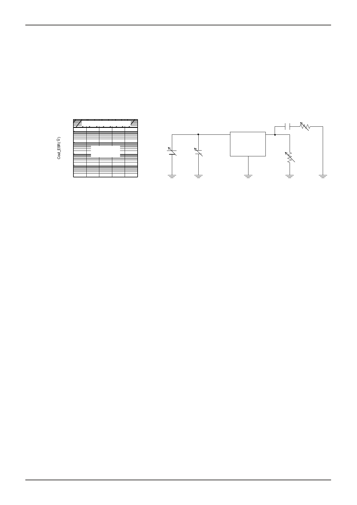
2. Output pins
It is necessary to place capacitors between each output pin and GND to prevent oscillation on the output. Usable
capacitance values range from 0.1µF ~ 1000µF. Abrupt fluctuations in input voltage and load conditions may affect the
output voltage. Output capacitance values should be determined only through sufficient testing of the actual application.
Vcc=5.6V~36V
Ta=-40℃~+125℃ Io=0A~500mA
Cin=0.33µF~100µF Cout=0.1µF~100µF
100
Unstable operating region
10
1
Stable operating
0.1
region
0.01
Vcc
(5.6~36V)
Cin
(0.33μF~)
Vcc
Vo
GND
Cout(0.1μF~)
ESR
(0.001Ω~)
Io(ROUT)
0.001
0
100 200 300 400 500
Cout_Io(mA)
ESR vs Io(reference data)
※Pin Settings / Precautions 2 Measurement circuit
3. CT pin
Connecting a capacitance of 0.01µF ~ 1µF on the CT pin is recommended.
www.rohm.com
© 2010 ROHM Co., Ltd. All rights reserved.
11/14
2010.11 - Rev.A
Share Link: 