BD12KA5W(2009) データシートの表示(PDF) - ROHM Semiconductor
部品番号
コンポーネント説明
一致するリスト
BD12KA5W Datasheet PDF : 10 Pages
| |||
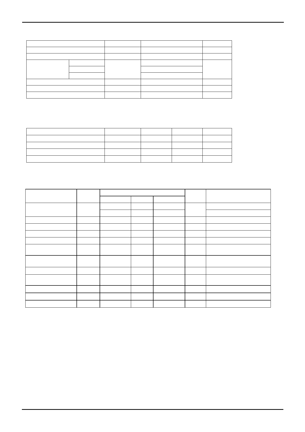
BD□□KA5,BD□□KA5W Series,BD00KA5W Series
Technical Note
●Block diagrams, Standard circuit examples
[BD00KA5WFP]
Vref
GND(FIN)
Driver
*Output voltage configuration
VOUT=VADJ×(R1+R2)÷R1(V)
:VADJ=0.75V(Typ.)
:A value of approximately 30kΩ
is recommended for R1.
TSD
OCP
Vcc (2PIN)
OUT (4PIN)
CTL (1PIN)
N.C.(3PIN)
1μF
1μF
R2
ADJ(5PIN)
R1
Fig.13
TO252-5(BD00KA5WFP)
Pin No.
PinName
Function
1
CTL
Output voltage ON/OFF control
2
Vcc
Power supply voltage input
3
N.C.
Unconnected terminal
4
OUT
Voltage output
5
ADJ
Output voltage configuration terminal
FIN
GND
GND
[BD□□KA5WFP]
GND(FIN)
Vref
Driver
R2
R1
TSD
OCP
Vcc (2PIN)
OUT (4PIN)
CTL (1PIN)
N.C.(3PIN)
N.C.(5PIN)
1μF
1μF
Fig.14
TO252-5(BD□□KA5WFP)
Pin No.
Pin Name
Function
1
CTL
Output voltage ON/OFF control
2
Vcc
Power supply voltage input
3
N.C.
Unconnected terminal
4
OUT
Voltage output
5
N.C.
Unconnected terminal
FIN
GND
GND
TOP VIEW
FIN
3
12 4 5
TO252-5
TOP VIEW
FIN
3
12 4 5
TO252-5
Vref
Driver
R2
R1
TSD
OCP
N.C.(2PIN)
Vcc (1PIN)
OUT (3PIN)
1μF
1μF
Fig.15
TO252-5(BD□□KA5FP)
Pin No.
Pin Name
1
Vcc
2
N.C.
3
OUT
FIN
GND
Function
Power supply voltage input
Unconnected terminal
Voltage output
GND
TOP VIEW
FIN
2
1
3
TO252-3
[BD00KA5WF]
1μF
Vcc(8PIN)
GND(7PIN)
GND(6PIN) CTL (5PIN)
Vref
Driver
*Output voltage configuration
OUT(1PIN)
TSD
OCP
VOUT=VADJ×(R1+R2)÷R1(V)
:VADJ=0.75V(Typ.)
:A value of approximately 30kΩ
is recommended for R1.
1μF
ADJ(2PIN)
R2 R1
N.C.(3PIN) N.C.(4IN)
Fig.16
SOP8(BD00KA5WF)
Pin No.
Pin Name
1
OUT
2
ADJ
3
N.C.
4
5
CTL
6
7
GND
8
Vcc
Function
Voltage output
Output voltage configuration terminal
Unconnected terminal
Output voltage ON/OFF control
GND
Power supply voltage input
TOP VIEW
85
14
SOP8
[BD□□KA5WF]
1μF
Vcc(8PIN)
GND(7PIN)
GND(6PIN) CTL (5PIN)
Vref
Driver
TSD
OUT(1PIN)
OCP
R2
R1
N.C.(3PIN)
N.C.(3PIN) N.C.(4IN)
1μF
Fig.17
SOP8(BD□□KA5WF)
Pin No.
1
2
3
4
5
6
7
8
Pin Name
OUT
N.C.
CTL
GND
Vcc
Function
Voltage output
Unconnected terminal
Output voltage ON/OFF control
GND
Power supply voltage input
TOP VIEW
85
14
SOP8
N.C. pins are electrically open to the inside of the IC chip.
www.rohm.com
© 2009 ROHM Co., Ltd. All rights reserved.
4/9
2009.04 - Rev.A
Share Link: 