BD3004HFP データシートの表示(PDF) - ROHM Semiconductor
部品番号
コンポーネント説明
一致するリスト
BD3004HFP Datasheet PDF : 9 Pages
| |||
● Detection voltage adjustment
OUT
R4
Vs Detection voltage
1,25V(Typ.)
R3
R2=3.56MΩ
For a basic detection voltage of 4.1 V,
Vdet = Vs × (R1 + R2 / R1)
To change the detection voltage,
insert pull-down resistor R3 (with a resistance value lower than R1)
R1=1.56MΩ
between the Vs and GND pins, and pull-up resistor R4 (with a
resistance value lower than R2) between the Vs and Vo pins.
Vdet = Vs × (R3 + R4 / R3) [R3<<R1, R4<<R2]
(All resistance values are typical ones.)
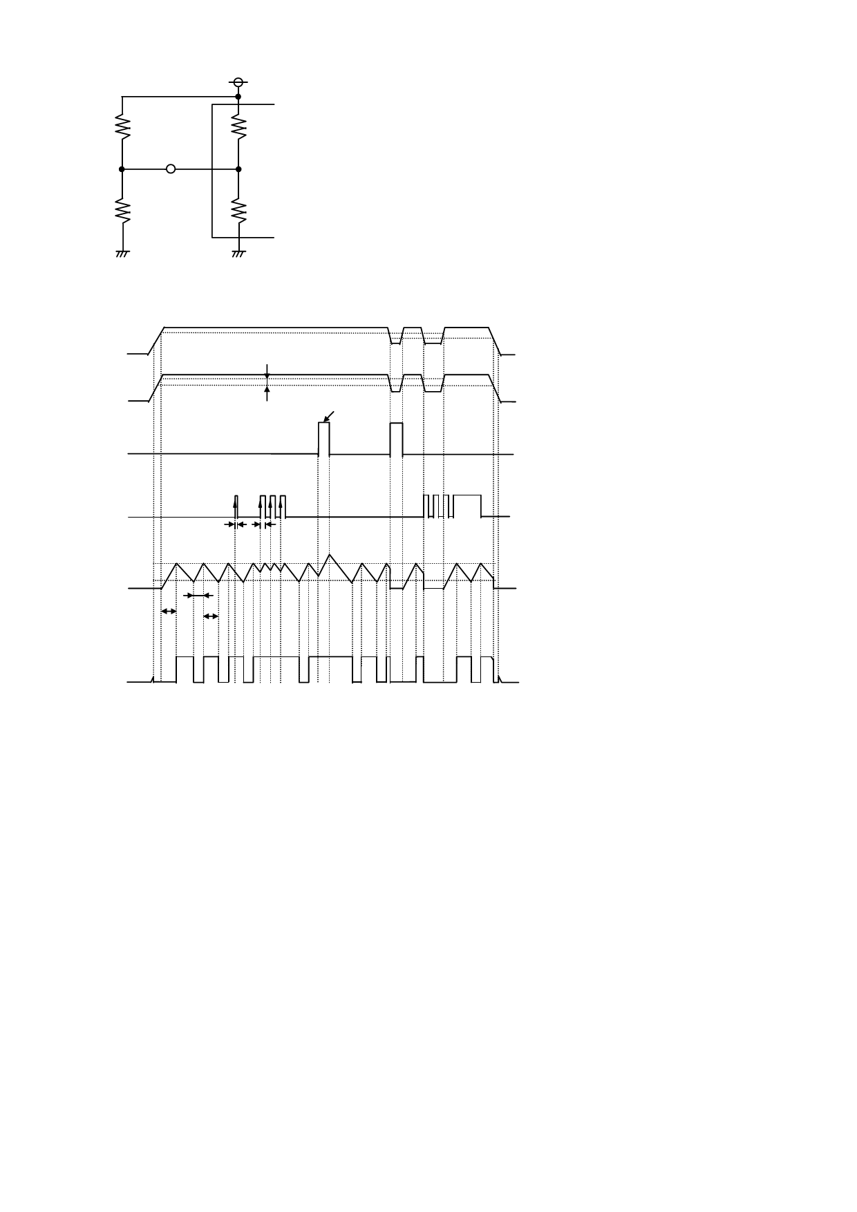
zTiming chart
Fig.15
Vcc
0
VOUT
VdetH
Vdet
0
VINH
0
When VINH = high
WDT current off
VHS
VdetH = Vdet + VHS
CLK
0
TWCLK TWCLK
VthH
VCT0VthL
TWL
TdLH TWH
RESET
0
(1)(2)(3) (4)(5) (6) (7)
(4)(5)(8)(9) (4)(5) (10)(2)(3)(10)(2)(3)(4)(5)(10)(11)
Fig.16
zExplanation
(1) When the output voltage (VOUT) reaches 1.0 V, the reset pin voltage (RESET) will switch to low level.
(2) When VOUT reaches or exceeds the reset clear voltage (VdetH), the external capacitor connected to the CT pin will begin to charge.
When the CT pin voltage (VCT) reaches the upper switching threshold voltage (VthH), RESET will maintain a low-level signal. When
VCT reaches the VthH voltage, RESET will switch from low to high level. The time from VCT reaching or exceeding the VdetH voltage
until RESET reverses (the RESET transmission delay time: TdLH) is given by the following equation:
TdLH (s) ≈ (1.26 × CT (µF)) / Icto (µA) [1]
(3) The watchdog timer operates when RESET rises.
(4) When VCT reaches the lower switching threshold voltage (VthL), the CT pin switches from discharging to charging, and RESET
switches from high level to low level. The watchdog timer reset time TWL is given by the following equation:
TWL(s) ≈ (1.02 × CT (µF)) / Icto (µA) [2]
(5) The CT pin state switches from charge to discharge when VCT reaches VthH, and RESET switches from low to high.
The watchdog timer monitor time TWH is given by the following equation:
TWH(s) ≈ (1.02 × CT (µF)) / Ictc (µA) [3]
(6) The CT pin state may not switche from charge to discharge when the CLK input pulse width (TWCLK) is short.
Use a TWCLK input pulse width of at least 500 ns.
(7) When a pulse (positive edge trigger) of at least 500 ns is input to the CLK pin while the CT pin is discharging, VCT switches from
discharging to charging and then switches back to discharging once it charges to VthH.
(8) Watchdog timer operation is forced off when the INH pin switches to high. At that time, only the watchdog timer will be turned off, and
reset detection will operate normally.
(9) The watchdog timer function turns on when the INH pin switches to low. At that time, the external capacitor on the CT pin will be
discharged.
(10) RESET switches from high to low when OUT falls to the RESET detection voltage (VDET) or lower.
(11) When VOUT falls to 0 V, the RESET signal stays low until VOUT reaches 1.0 V
5/8
Share Link: 