APL5325 データシートの表示(PDF) - Anpec Electronics
部品番号
コンポーネント説明
一致するリスト
APL5325 Datasheet PDF : 15 Pages
| |||
APL5325
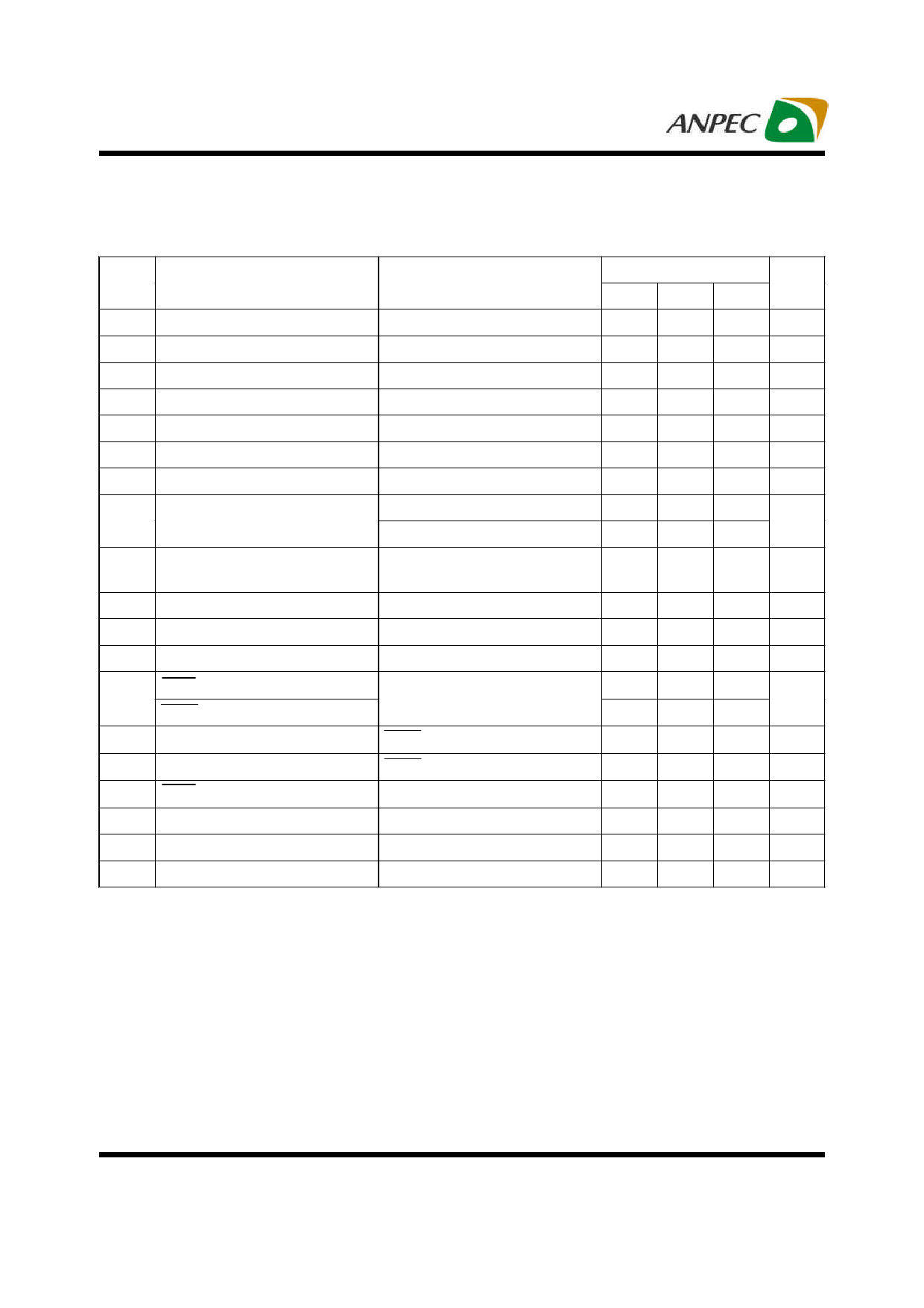
Electrical Characteristics
Unless otherwise specified, these specifications apply over VIN = VOUT+1V, IOUT=0~300mA, CIN = 1µF, COUT = 2.2µF, TA = -40 to 85oC.
Typical values are at TA = 25oC.
Symbol
Parameter
VIN Input Voltage
VOUT Output Voltage Range
IQ Quiescent Current
VREF Reference Voltage
Output Voltage Accuracy
REGLINE Line Regulation
REGLOAD Load Regulation
VDROP Dropout Voltage
Test Conditions
APL5325
Min. Typ. Max.
3
-
6
0.8
-
5.5
IOUT =10mA ~300mA
-
135
160
Measured on SET, VIN=3V, IOUT=10mA
-
0.8
-
IOUT=10mA
-2
-
+2
∆VOUT%/∆VIN, IOUT=10mA
-0.06
-
+0.06
∆VOUT%/∆IOUT
-0.2
-
+0.2
VOUT = 2.5V, IOUT = 300mA
-
500
650
VOUT = 3.3V, IOUT = 300mA
-
300
400
Unit
V
V
µA
V
%
%/V
%/A
mV
PSRR Power Supply Ripple Rejection Ratio f = 10kHz, IOUT = 300mA
-
45
-
dB
Noise
ILIMIT
ISHORT
Current Limit
Foldback Current
SHDN Input Voltage High
SHDN Input Voltage Low
VOUT Discharge MOSFET RDS(ON)
Shutdown VIN Supply Current
SHDN Pull Low Resistance
Over Temperature Threshold
Over Temperature Hysteresis
SET Input Bias Current
f = 80Hz to 100kHz, IOUT = 300mA
VOUT = 0V
SHDN = Low
SHDN = Low, VIN = 6V
VSET=0.8V
-
160
450
550
-
µVRMS
-
mA
-
80
-
mA
1.6
-
-
V
-
-
0.4
-
60
-
Ω
-
0.1
1
µA
-
3
-
MΩ
-
160
-
oC
-
40
-
oC
-100
-
100
nA
Copyright © ANPEC Electronics Corp.
3
Rev. A.1 - Nov., 2008
www.anpec.com.tw
Share Link: 