STK11C48-P25 データシートの表示(PDF) - Simtek Corporation
部品番号
コンポーネント説明
一致するリスト
STK11C48-P25 Datasheet PDF : 10 Pages
| |||
STK11C48
Internally, RECALL is a two-step procedure. First,
the SRAM data is cleared, and second, the nonvola-
tile information is transferred into the SRAM cells.
After the tRECALL cycle time the SRAM will once again
be ready for READ and WRITE operations. The
RECALL operation in no way alters the data in the
Nonvolatile Element cells. The nonvolatile data can
be recalled an unlimited number of times.
POWER-UP RECALL
During power up, or after any low-power condition
(VCC < VRESET), an internal RECALL request will be
latched. When VCC once again exceeds the sense
voltage of VSWITCH, a RECALL cycle will automatically
be initiated and will take tRESTORE to complete.
If the STK11C48 is in a WRITE state at the end of
power-up RECALL, the SRAM data will be corrupted.
To help avoid this situation, a 10K Ohm resistor
should be connected either between W and system
VCC or between E and system VCC.
HARDWARE PROTECT
The STK11C48 offers hardware protection against
inadvertent STORE operation during low-voltage
conditions. When VCC < VSWITCH, all software STORE
operations are inhibited.
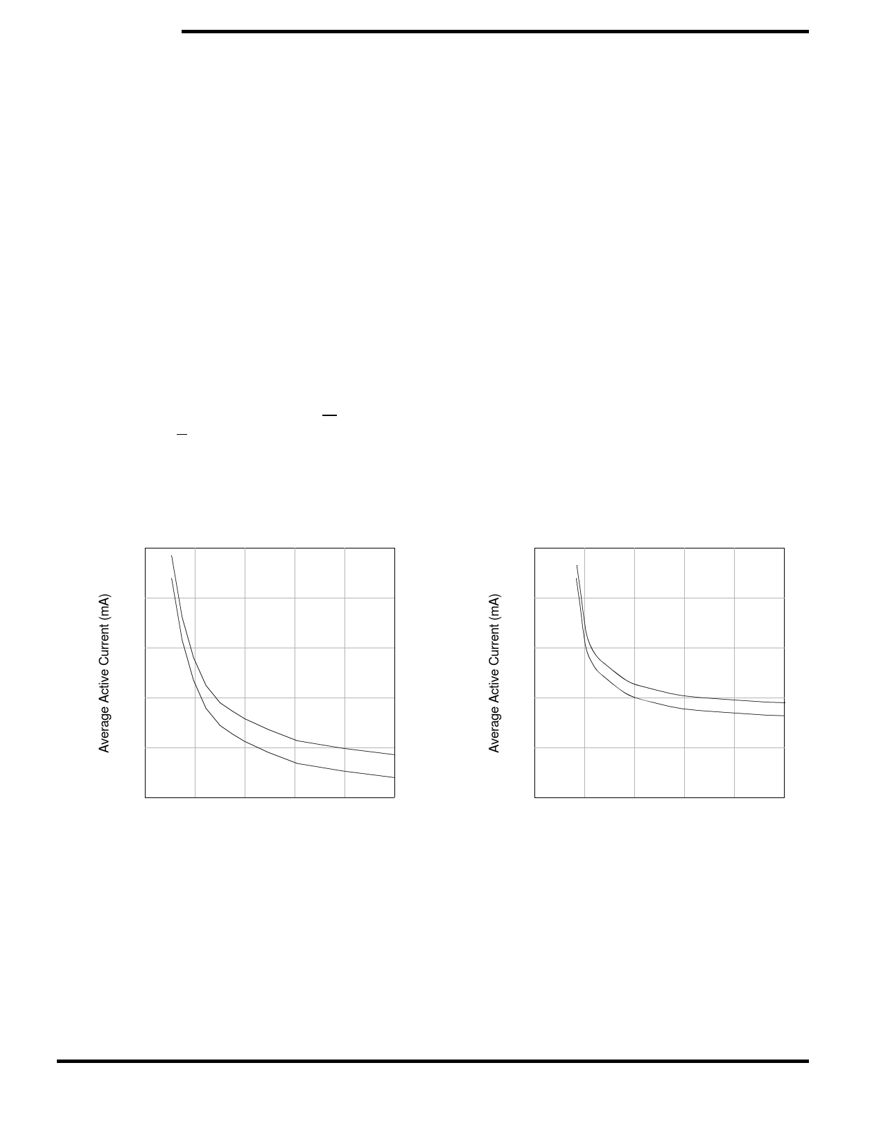
LOW AVERAGE ACTIVE POWER
The STK11C48 draws significantly less current
when it is cycled at times longer than 50ns. Figure 2
shows the relationship between ICC and READ cycle
time. Worst-case current consumption is shown for
both CMOS and TTL input levels (commercial tem-
perature range, VCC = 5.5V, 100% duty cycle on
chip enable). Figure 3 shows the same relationship
for WRITE cycles. If the chip enable duty cycle is
less than 100%, only standby current is drawn
when the chip is disabled. The overall average cur-
rent drawn by the STK11C48 depends on the fol-
lowing items: 1) CMOS vs. TTL input levels; 2) the
duty cycle of chip enable; 3) the overall cycle rate
for accesses; 4) the ratio of READs to WRITEs; 5)
the operating temperature; 6) the Vcc level; and 7) I/
O loading.
100
100
80
80
60
40
TTL
20
CMOS
0
50
100 150 200
Cycle Time (ns)
Figure 2: ICC (max) Reads
60
TTL
40
CMOS
20
0
50
100 150 200
Cycle Time (ns)
Figure 3: ICC (max) Writes
March 2006
8Document Control # ML0003 rev 0.2
Share Link: 