AP5004 データシートの表示(PDF) - Diodes Incorporated.
部品番号
コンポーネント説明
一致するリスト
AP5004 Datasheet PDF : 10 Pages
| |||
AP5004
PWM CONTROL 2.5A STEP-DOWN CONVERTER
Electrical Characteristics (VIN = 12V, TA=25°C, unless otherwise specified)
Symbol
Parameter
Conditions
Min
VFB
Feedback Voltage
VIN
Input Voltage
ISTBY Standby Current
VEN =0V
∆VOUT/VOUT Line Regulation
VIN = 10V~32V
∆VOUT/VOUT Load Regulation
IOUT = 0.1 to 2.5A
fOSC Oscillation Frequency
Measure waveform at SW pin
fOSC1
Frequency of Current Limit or
Short Circuit Protect
Measure waveform at SW pin
DC
Maximum Duty Cycle
Minimum Duty Cycle
VFB =0.5V
VFB =1.0V
VIH EN Pin Logic Input Threshold Regulator ON
VIL
Voltage
Regulator OFF
ISH
ISL
EN Pin Input Leakage Current
RDS(ON) Internal MOSFET RDS(ON)
ILIMIT Current Limit
η
Efficiency
VIN = 12V, VOUT = 5V, IOUT = 2.5A
θJA
Thermal Resistance
Junction-to-Ambient
SOP-8L (Note 3)
θJC
Thermal Resistance
Junction-to-Case
SOP-8L (Note 3)
0.780
10
-
-
-
240
-
-
-
2.0
-
-
-
-
3.5
-
-
-
Notes: 3. Test condition for SOP-8L: Device mounted on 2oz copper, minimum recommended pad layout, FR-4 PCB.
Typ.
0.8
-
2
±1.0
1
300
50
90
0
-
-
20
-10
80
-
90
124
25
Max Unit
0.820 V
32 V
- µA
±1.5 %/V
1.5 %
360 KHz
- KHz
-
%
-
%
-
0.8
V
- µA
- µA
120 mΩ
-
A
-
%
- oC/W
- oC/W
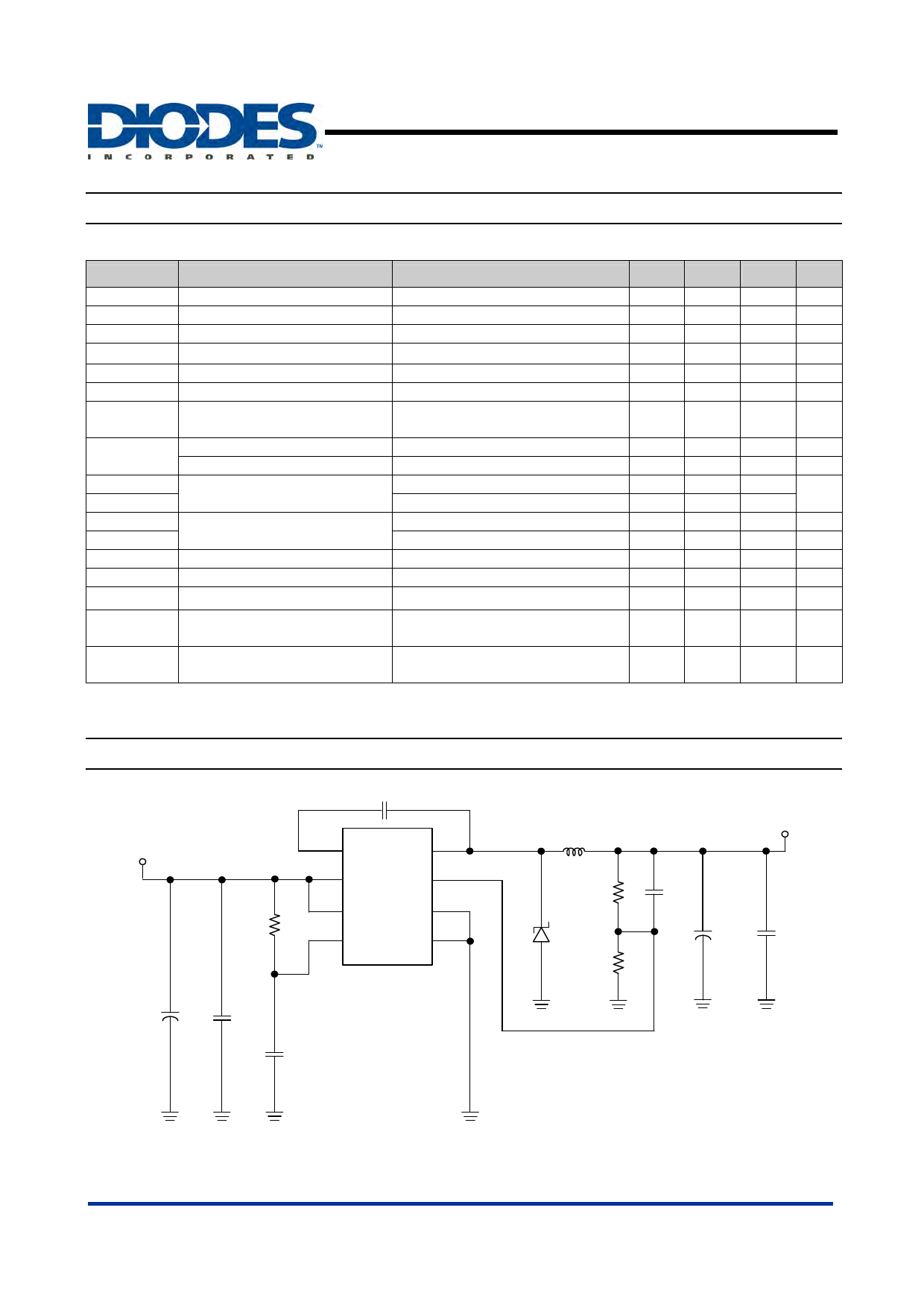
Typical Application Circuit
C7 0.1uF
U1
VIN
3 Vboost
4
Output
R5
100K
5 VCC
2
FB
AP5004
6 VCC
GND 7
1
EN
8
GND
C2
220uF/63V
C3
0.1uF
C6
0.1uF
L1-(WURTH 744132)
1 33uH 2
VOUT = 5V
R1
685ohm
D1
B340
R2
130ohm
C1
100pF
C4
470uF/16V
C5
0.1uF
Notes:
Note : V OUT = VFB x (1+R1/R2)
R B = 100 ~ 300 ohm
4. Suggested DIODES Power Schottky P/N: PDS540 or B540C.
AP5004 Rev. 3
4 of 10
www.diodes.com
JUNE 2008
© Diodes Incorporated
Share Link: 