AK4563A データシートの表示(PDF) - Asahi Kasei Microdevices
部品番号
コンポーネント説明
一致するリスト
AK4563A Datasheet PDF : 39 Pages
| |||
ASAHI KASEI
[AK4563A]
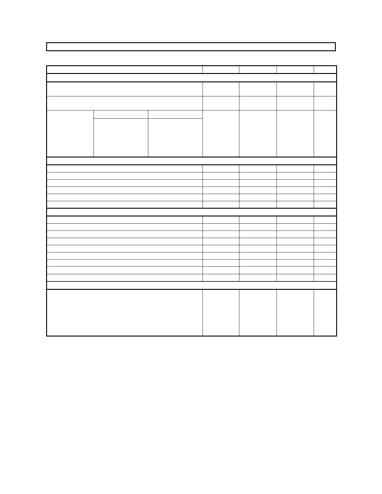
ANALOG CHARACTERISTICS
(Ta=25°C; VA, VD, VT=2.5V; fs=48kHz; Signal Frequency =1kHz; Measurement frequency = 10Hz ∼ 20kHz;
S/(N+D), D-Range and S/N are value against Full-scale; Unless otherwise specified)
Parameter
min
typ
max
Units
Input PGA Characteristics (IPGA):
Input Voltage
(INTL1-0, INTR1-0, EXTL, EXTR, LIN, RIN pins) (Note 5)
1.35
1.5
1.65
Vpp
Input Resistance: MIC (INTL1-0,INTR1-0,EXTL,EXTR pins)
LINE (LIN, RIN pins)
6.5
80
10
125
14.5
176
kΩ
Step Size
(Note 6)
MIC
LINE
+28dB ∼ -8dB
+6dB ∼ -30dB
0.1
0.5
0.9
dB
-8dB ∼ -16dB
-30dB ∼ -38dB
0.1
1
1.9
dB
-16dB ∼ -32dB
-38dB ∼ -54dB
0.1
2
3.9
dB
-32dB ∼ -40dB
-54dB ∼ -62dB
-
2
-
dB
-40dB ∼ -52dB
-62dB ∼ -74dB
-
4
-
dB
ADC Analog Input Characteristics: (Note 7)
Resolution
S/(N+D)
(-2dBFS Input)
D-Range
(EIAJ)
S/N
(EIAJ)
Interchannel Isolation
Interchannel Gain Mismatch
16
Bits
74
83
dB
81
87
dB
81
87
dB
85
100
dB
0.2
0.5
dB
DAC Analog Output Characteristics: Measured by LOUT/ROUT
Resolution
S/(N+D)
(0dBFS Input)
D-Range
(EIAJ)
S/N
(EIAJ)
Interchannel Isolation
Interchannel Gain Mismatch
Output Voltage (Note 8)
Load Resistance
Load Capacitance
16
Bits
77
86
dB
85
91
dB
85
91
dB
85
100
dB
0.2
0.5
dB
1.35
1.5
1.65
Vpp
10
kΩ
20
pF
Power Supplies
Power Supply Current: VA+VD+VT
Normal Operation (PDN= “H”)
All Power ON (PM4-0= “1”)
IPGA0+ADC0+IPGA1+ADC1 (PM3-0= “1”)
DAC (PM4= “1”)
Power-down mode (PDN= “L”) (Note 9)
18
27
mA
-
13.5
-
mA
-
5.5
-
mA
10
100
µA
Note 5. Full-scale voltage of analog inputs when IPGA0 and IPGA1 bits are “0” and are set to 0dB. Its voltage is
proportional to VREF. Vin = 0.6 x VREF.
Note 6. IPGA1 does not have a gain table of LINE side.
Note 7. ADC0 is input from INTL0/INTR0 or EXTL/EXTR or LIN/RIN and it measures included in IPGA0. The gain of
IPGA0 is set 0dB. ADC1 is input from INTL1/INTR1 and it measures included in IPGA1. The gain of IPGA1 is
set 0dB.
DC-offset in “IPGA0+ADC0” and “IPGA1+ADC1” are cancelled by internal HPF.
Note 8. Analog output voltage is proportional to VREF. Vout = 0.6 x VREF.
Note 9. All digital input pins except for PDN pin are held VT or DGND, and PDN pin is held DGND.
MS0067-E-02
-6-
2004/12
Share Link: 