ADXL346 データシートの表示(PDF) - Analog Devices
部品番号
コンポーネント説明
一致するリスト
ADXL346 Datasheet PDF : 40 Pages
| |||
ADXL346
PIN CONFIGURATION AND FUNCTION DESCRIPTIONS
VDD I/O 1
NC 2
NC 3
16 15 14
ADXL346
+X
SCL/SCLK 4 +Y
NC 5
6
+Z
7
8
NC = NO INTERNAL
CONNECTION
13 GND
12 GND
11 INT1
10 NC
9 INT2
TOP VIEW
(Not to Scale)
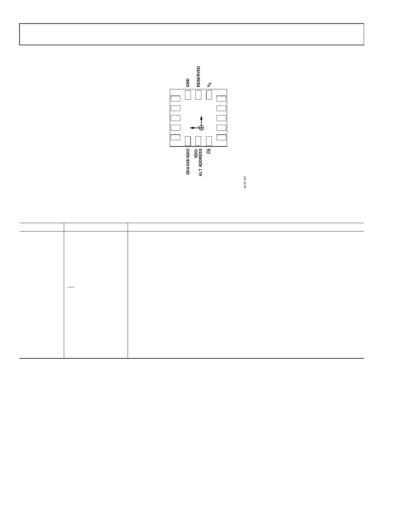
Figure 3. Pin Configuration (Top View)
Table 5. Pin Function Descriptions
Pin No.
Mnemonic
1
VDD I/O
2
NC
3
NC
4
SCL/SCLK
5
NC
6
SDA/SDI/SDIO
7
SDO/ALT ADDRESS
8
CS
9
INT2
10
NC
11
INT1
12
GND
13
GND
14
VS
15
RESERVED
16
GND
Description
Digital Interface Supply Voltage.
Not Internally Connected.
Not Internally Connected.
Serial Communications Clock.
Not Internally Connected.
Serial Data (I2C)/Serial Data Input (SPI 4-Wire)/Serial Data Input and Output (SPI 3-Wire).
Serial Data Output (SPI 4-Wire)/Alternate I2C Address Select (I2C).
Chip Select.
Interrupt 2 Output.
Not Internally Connected.
Interrupt 1 Output.
Must be connected to ground.
Must be connected to ground.
Supply Voltage.
Reserved. This pin must be connected to VS.
Must be connected to ground.
Rev. 0 | Page 6 of 40
Share Link: 