ADSP-2195MKCA-160X データシートの表示(PDF) - Analog Devices
部品番号
コンポーネント説明
一致するリスト
ADSP-2195MKCA-160X Datasheet PDF : 68 Pages
| |||
35(/,0,1$5< 7(&+1,&$/ '$7$
September 2001 For current information contact Analog Devices at 800/262-5643
ADSP-2195
within 64K word boundaries of each of the 256 memory
pages, but these buffers may not cross page boundaries.
Secondary registers duplicate all the primary registers in the
DAGs; switching between primary and secondary registers
provides a fast context switch.
Efficient data transfer in the core is achieved with the use of
internal buses:
• Program Memory Address (PMA) Bus
• Program Memory Data (PMD) Bus
• Data Memory Address (DMA) Bus
• Data Memory Data (DMD) Bus
• DMA Address Bus
• DMA Data Bus
The two address buses (PMA and DMA) share a single
external address bus, allowing memory to be expanded
off-chip, and the two data buses (PMD and DMD) share a
single external data bus. Boot memory space and I/O
memory space also share the external buses.
Program memory can store both instructions and data, per-
mitting the ADSP-2195 to fetch two operands in a single
cycle, one from program memory and one from data
memory. The DSP’s dual memory buses also let the
ADSP-219x core fetch an operand from data memory and
the next instruction from program memory in a single cycle.
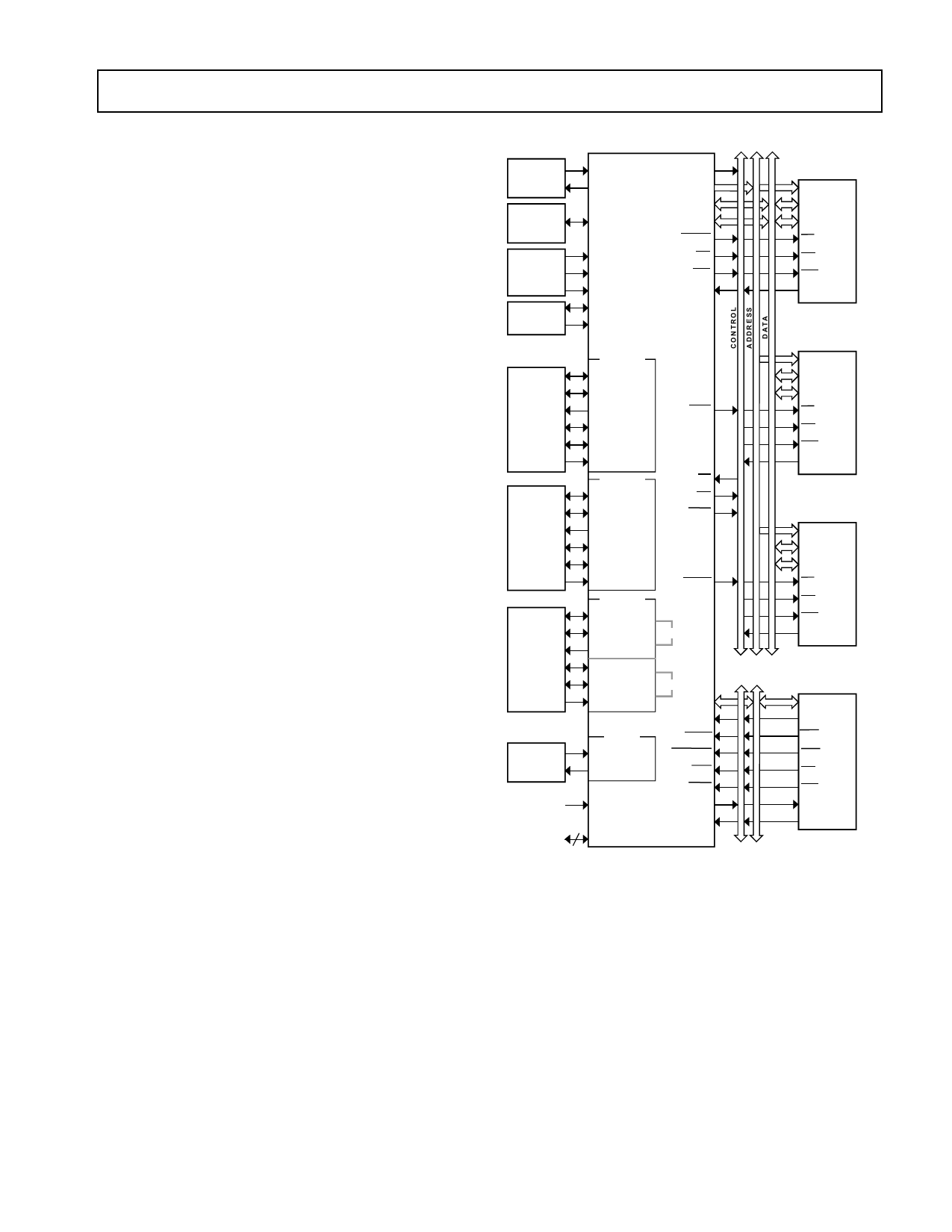
DSP Peripherals Architecture
The functional block diagram on page 1 shows the DSP’s
on-chip peripherals, which include the external memory
interface, Host port, serial ports, SPI-compatible ports,
UART port, JTAG test and emulation port, timers, flags,
and interrupt controller. These on-chip peripherals can
connect to off-chip devices as shown in Figure 1.
The ADSP-2195 has a 16-bit Host port with DMA capa-
bility that lets external Hosts access on-chip memory. This
24-pin parallel port consists of a 16-pin multiplexed
data/address bus and provides a low-service overhead data
move capability. Configurable for 8- or 16-bits, this port
provides a glueless interface to a wide variety of 8- and 16-bit
microcontrollers. Two chip-selects provide Hosts access to
the DSP’s entire memory map. The DSP is bootable
through this port.
The ADSP-2195 also has an external memory interface that
is shared by the DSP’s core, the DMA controller, and DMA
capable peripherals, which include the UART, SPORT0,
SPORT1, SPORT2, SPI0, SPI1, and the Host port. The
external port consists of a 16-bit data bus, a 22-bit address
bus, and control signals. The data bus is configurable to
provide an 8 or 16 bit interface to external memory. Support
for word packing lets the DSP access 16- or 24-bit words
from external memory regardless of the external data bus
width. When configured for an 8-bit interface, the unused
&/2&.
25
&5<67$/
7,0(5
287 25
&$3785(
&/2&.
0 8 /7 ,3 /<
$1'
5$1*(
%227
$1' 23
02'(
$ ' 6 3
&/ . ,1
&/.287
;7$/
$''5±
'$7$±
70 5±
'$7$±
06±
06 ( / ±3 )±
5'
') 3 )
:5
%< 3$ 6 6
$&.
%0 2 '( ±
2302'(
63257
7& / .
7) 6
6(5,$/
'(9,&(
2 3 7,2 1 $ /
'7
5&/.
5)6
%06
'5
63257
%5
7& / .
%*
6(5,$/
'(9,&(
2 3 7,2 1 $ /
7) 6
'7
5&/.
5)6
%*+
'5
,20 6
63257
7& / . 6 & .
7)60 26 , 63 ,
6(5,$/
'(9,&(
2 3 7,2 1 $ /
'7 0 ,6 2
5& / . 6 & .
5)602 6, 63 ,
'5 0 ,62
+$'±
+$
8$57
'(9,&(
2 3 7,2 1 $ /
8$57
5; '
7; '
+&06
+&,20 6
+5'
+:5
5( 6( 7
+$&.
-7 $ *
+$ / (
+$&.B3
(;7(51$/
0(025<
2 3 7,2 1 $ /
$''5±
'$7$±
'$7$±
&6
2(
:(
$&.
%2 2 7
0(025<
2 3 7,2 1 $ /
$''5±
'$7$±
'$7$±
&6
2(
:(
$&.
(;7(51$/
,2 0( 025<
2 37,2 1 $/
$''5±
'$7$±
'$7$±
&6
2(
:(
$&.
+267
35 2 &( 6 6 2 5
2 37,2 1 $/
$''5±
'$7$±
$''5
&6
&6
5'
:5
$&.
$/(
Figure 1. ADSP-2195 System Diagram
eight lines provide eight programmable, bidirectional gen-
eral-purpose Programmable Flag lines, six of which can be
mapped to software condition signals.
The memory DMA controller lets the ADSP-2195 move
data and instructions from between memory spaces: inter-
nal-to-external, internal-to-internal, and external-to-
external. On-chip peripherals can also use this controller for
DMA transfers.
The ADSP-2195 can respond to up to seventeen interrupts
at any given time: three internal (stack, emulator kernel, and
power-down), two external (emulator and reset), and twelve
user-defined (peripherals) interrupts. Programmers assign
REV. PrA
This information applies to a product under development. Its characteristics and specifications are subject to change with-
5
out notice. Analog Devices assumes no obligation regarding future manufacturing unless otherwise agreed to in writing.
Share Link: 