ADSP-2185NKCA-320 データシートの表示(PDF) - Analog Devices
部品番号
コンポーネント説明
一致するリスト
ADSP-2185NKCA-320 Datasheet PDF : 45 Pages
| |||
ADSP-218xN Series
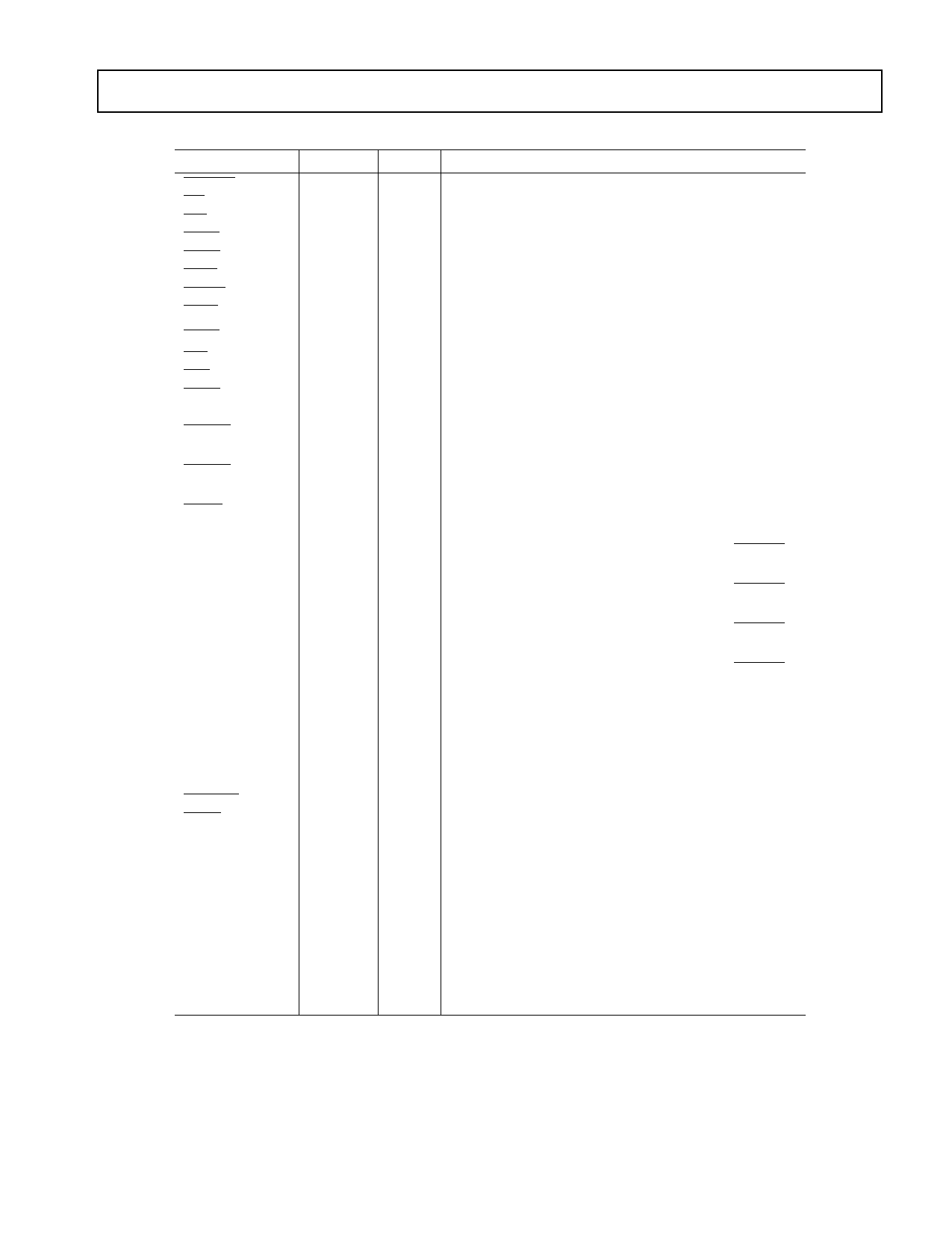
Table 2. Common-Mode Pins
Pin Name
# of Pins I/O
Function
RESET
BR
BG
BGH
DMS
PMS
IOMS
BMS
1
I
Processor Reset Input
1
I
Bus Request Input
1
O
Bus Grant Output
1
O
Bus Grant Hung Output
1
O
Data Memory Select Output
1
O
Program Memory Select Output
1
O
Memory Select Output
1
O
Byte Memory Select Output
CMS
1
RD
1
WR
1
IRQ2
1
PF7
IRQL1
1
PF6
IRQL0
1
PF5
IRQE
1
PF4
Mode D
1
PF3
Mode C
1
PF2
Mode B
1
PF1
Mode A
1
PF0
CLKIN
1
XTAL
1
CLKOUT
1
SPORT0
5
SPORT1
5
IRQ1–0, FI, FO
PWD
1
PWDACK
1
FL0, FL1, FL2 3
VDDINT
2
VDDEXT
4
GND
10
VDDINT
4
VDDEXT
7
GND
20
EZ-Port
9
O
Combined Memory Select Output
O
Memory Read Enable Output
O
Memory Write Enable Output
I
Edge- or Level-Sensitive Interrupt Request1
I/O
Programmable I/O pin
I
Level-Sensitive Interrupt Requests1
I/O
Programmable I/O Pin
I
Level-Sensitive Interrupt Requests1
I/O
Programmable I/O Pin
I
Edge-Sensitive Interrupt Requests1
I/O
Programmable I/O Pin
I
Mode Select Input—Checked Only During RESET
I/O
Programmable I/O Pin During Normal Operation
I
Mode Select Input—Checked Only During RESET
I/O
Programmable I/O Pin During Normal Operation
I
Mode Select Input—Checked Only During RESET
I/O
Programmable I/O Pin During Normal Operation
I
Mode Select Input—Checked Only During RESET
I/O
Programmable I/O Pin During Normal Operation
I
Clock Input
O
Quartz Crystal Output
O
Processor Clock Output
I/O
Serial Port I/O Pins
I/O
Serial Port I/O Pins
Edge- or Level-Sensitive Interrupts, FI, FO2
I
Power-Down Control Input
O
Power-Down Acknowledge Control Output
O
Output Flags
I
Internal VDD (1.8 V) Power (LQFP)
I
External VDD (1.8 V, 2.5 V, or 3.3 V) Power (LQFP)
I
Ground (LQFP)
I
Internal VDD (1.8 V) Power (Mini-BGA)
I
External VDD (1.8 V, 2.5 V, or 3.3 V) Power (Mini-
BGA)
I
Ground (Mini-BGA)
I/O
For Emulation Use
1Interrupt/Flag pins retain both functions concurrently. If IMASK is set to enable the corresponding interrupts, the DSP will
vector to the appropriate interrupt vector address when the pin is asserted, either by external devices or set as a programmable
flag.
2SPORT configuration determined by the DSP System Control Register. Software configurable.
REV. 0
–5–
Share Link: 