ADSP-21261 データシートの表示(PDF) - Analog Devices
部品番号
コンポーネント説明
一致するリスト
ADSP-21261 Datasheet PDF : 48 Pages
| |||
SHARC
Embedded Processor
ADSP-21261/ADSP-21262/ADSP-21266
SUMMARY
High performance 32-bit/40-bit floating-point processor
optimized for high performance audio processing
Code compatibility—at assembly level, uses the same
instruction set as other SHARC DSPs
Processes high performance audio while enabling low
system costs
Audio decoders and postprocessor algorithms support
nonvolatile memory that can be configured to contain a
combination of PCM 96 kHz, Dolby Digital, Dolby Digital
Surround EX, DTS-ES Discrete 6.1, DTS-ES Matrix 6.1, DTS
96/24 5.1, MPEG2 AAC LC, MPEG2 BC 2ch, WMA-
PRO V7.1, Dolby Pro Logic II, Dolby Pro Logic 2x, and
DTS Neo:6
Various multichannel surround sound decoders are con-
tained in ROM. For configurations of decoder algorithms,
see Table 3 on Page 4.
Single-instruction multiple-data (SIMD) computational archi-
tecture—two 32-bit IEEE floating-point/32-bit fixed-point/
40-bit extended precision floating-point computational
units, each with a multiplier, ALU, shifter, and register file
High bandwidth I/O—a parallel port, an SPI port, 6 serial
ports, a Digital application interface (DAI), and JTAG
DAI incorporates two precision clock generators (PCGs), an
input data port (IDP) that includes a parallel data acquisi-
tion port (PDAP), and 3 programmable timers, all under
software control by the signal routing unit (SRU)
On-chip memory—up to 2M bits on-chip SRAM and a dedi-
cated 4M bits on-chip mask-programmable ROM
The ADSP-2126x processors are available with a 150 MHz or a
200 MHz core instruction rate. For complete ordering
information, see Ordering Guide on Page 45.
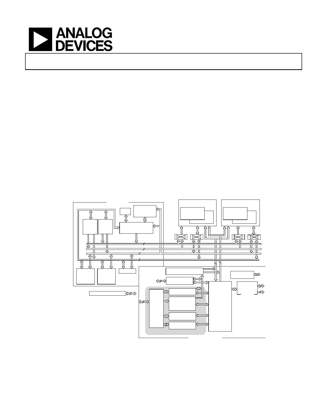
CORE PROCESSOR
TIME R
INSTRUCTION
CACHE
32 ؋ 48-BIT
DAG1
DAG2
8 ؋ 4 ؋ 32 8 ؋ 4 ؋ 32
PROG RAM
SEQ UENCER
DUAL PORTED MEMORY
BLOCK 0
S RAM
1M BIT
ROM
2M BIT
ADDR
DATA
DUAL PORTED MEMORY
BLO CK 1
S RAM
1M BIT
ROM
2M BIT
ADDR
DATA
PM ADDRESS BUS
32
DM ADDRESS BUS
32
PROCES SING
ELEMENT
( PEX )
PRO CESSING
ELEMENT
( PE Y)
PX REGI STER
6
JTAG TEST & EMULATION
S
64 PM DATA BUS
64 DM DATA BUS
I OD
IOA
( 32 )
( 19 )
DMA CONTRO LLER
2 2 C HA N N ELS
4
SPI PORT (1)
SERIAL PORTS (6)
20
SI GNAL
RO UTI NG
UNI T
I NP UT
DATA PORTS (8)
PARALLEL DATA
ACQUISITION PORT
PRECISION CLOCK
GENERATORS (2)
3
PE RIPHERAL
TIMERS (3)
4
GPIO FLAGS/
IRQ /TIMEXP
IOP
RE GISTE RS
(MEMORY MAPPED)
CO NTROL,
S TATUS ,
DATA BUFFERS
16
AD D R ES S/
D A TA BU S / GPIO
3
CON TR OL/GPIO
P ARALLEL
P ORT
DIGITAL AUDIO INTERFACE
I/O PROCESSOR
Figure 1. Functional Block Diagram
SHARC and the SHARC logo are registered trademarks of Analog Devices, Inc.
Rev. G
Document Feedback
Information furnished by Analog Devices is believed to be accurate and reliable.
However, no responsibility is assumed by Analog Devices for its use, nor for any
infringements of patents or other rights of third parties that may result from its use.
Specifications subject to change without notice. No license is granted by implication
or otherwise under any patent or patent rights of Analog Devices. Trademarks and
registered trademarks are the property of their respective owners.
One Technology Way, P.O. Box 9106, Norwood, MA 02062-9106 U.S.A.
Tel: 781.329.4700
©2012 Analog Devices, Inc. All rights reserved.
Technical Support
www.analog.com
Share Link: 