AD8346_ データシートの表示(PDF) - Analog Devices
部品番号
コンポーネント説明
一致するリスト
AD8346_ Datasheet PDF : 8 Pages
| |||
Application Note
AN-1039
After low-pass filtering, the two word streams are applied to a
pair of digital-to-analog converters (DAC). The DAC outputs
drive two low-pass filters whose primary role is to remove
Nyquist images. The outputs of these filters then drive the
baseband inputs of the IQ modulator. The local oscillator (LO)
input of the modulator is driven by a relatively pure CW signal
generated by a phase-locked loop (PLL) such as the ADF4106
from Analog Devices, Inc. Now, take a closer look at the
operation of the IQ modulator.
The LO signal is split into two signals, equal in amplitude but
with a phase difference of exactly 90°. These two quadrature
signals drive the inputs of the two mixers that, for the purposes
of this application note, are viewed as analog multipliers. The
outputs of these two multipliers are added together (in the
Σ block of the IQ modulator) to provide the IQ modulator’s
output.
While it is apparent that the baseband data streams have
been filtered, instead briefly consider them as the original bit
streams. Instead of a stream of 1s and 0s, think of them as two
streams switching between a value of +1 and –1. So, the output
of the I multiplier consists of a vector which is flipping in-phase
between 0° and 180°as the bit stream alternates. Likewise, the
output of the Q multiplier is a vector that flips between +90°
and –90° as the bit stream modulates the original 90° vector.
Thus, if at a particular instant, both the I and Q bit streams are
equal to +1, the result at the output of the IQ modulator is the
sum of the 90° and 0° vectors, that is, a +45° vector. Likewise,
I and Q bit combinations of −1/+1, −1/−1, and +1/−1 produce
vectors (commonly called symbols) all of equal amplitude at
+135°, −135°, and −45°, respectively. If these vectors were
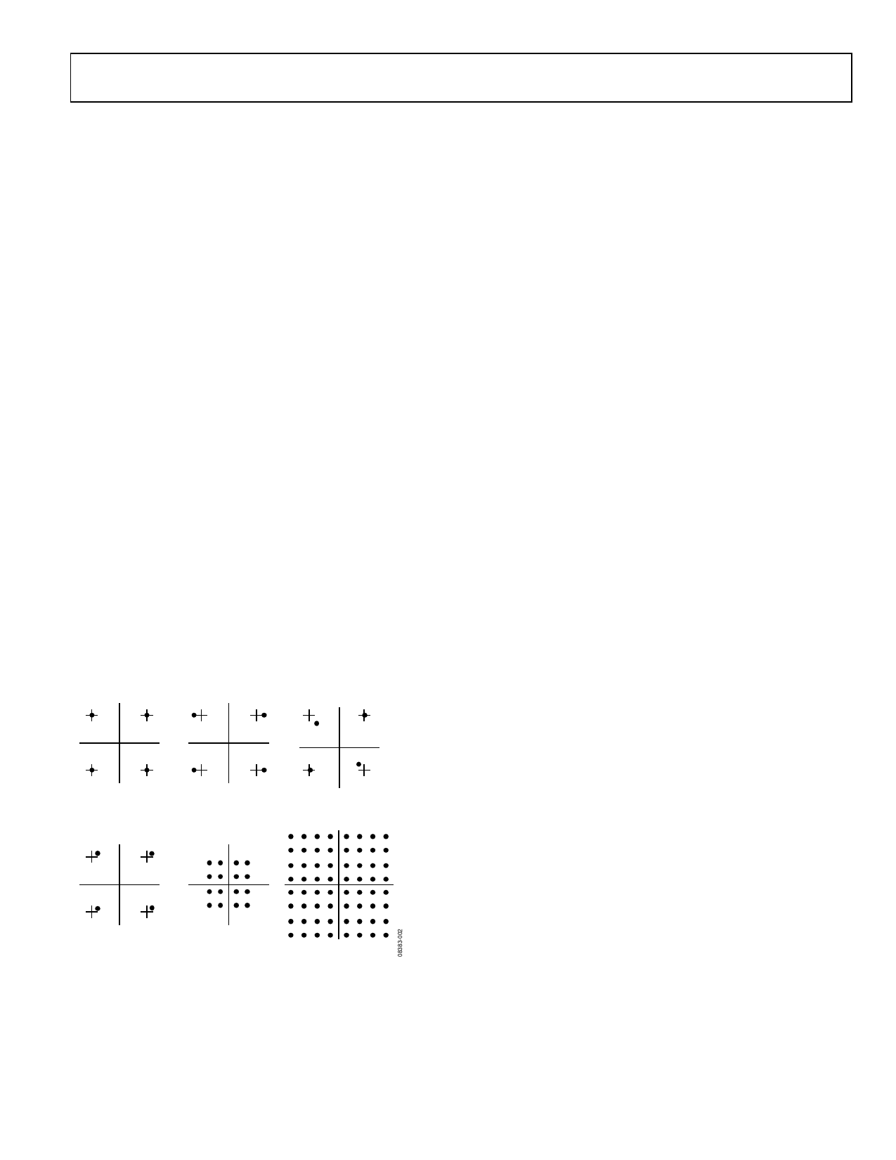
plotted, observe the constellation of the modulated carrier
(see Figure 2A).
(A)
(B)
(C)
(D)
(E)
(F)
Figure 2. Error Vector Magnitude Constellations that Result from Various
Modulator Imperfections
MODULATOR IMPERFECTIONS
Contrary to the previous hypothetical situation, in a real IQ
modulator, things do not look so perfect. A series of effects in
the IQ modulator conspire to create QPSK (or QAM) vectors
that are neither equal in amplitude nor separated by exactly 45°.
Consider first what happens if for some reason the gain of the I
path is greater than that of the Q channel; this could be caused
by a DAC gain mismatch, low-pass filter insertion loss, mismatch,
or gain imbalance inside the IQ modulator. Regardless of where
this gain imbalance comes from, its effect is the same. Because
the 0°/180° vectors at the output of the I multiplier are larger
than the +90°/−90° vectors from the Q multiplier, the shape
of the constellation becomes rectangular (see Figure 2B). This
degrades signal integrity at the receiver because the receiver is
expecting a perfectly square constellation. In the QPSK example
shown in Figure 2B, a slight gain imbalance is unlikely to result
in an incorrect bit decision in the receiver unless the received
signal is very small. However, in higher order modulation
schemes such as 16 QAM or 64 QAM (see Figure 2E and
Figure 2F), the increased density of the constellation points
could easily combine with an IQ gain imbalance to produce
an incorrect symbol decision in the receiver.
In most IQ modulators, the 90° phase split of the LO is achieved
using either a polyphase filter or a divide-by-two flip-flop circuit
(which requires an external LO that is twice the desired output
frequency). In either circuit, the 90° phase split or quadrature is
never perfect. For example, if there is a 1° quadrature error, the
shape of the resulting constellation is slightly trapezoidal (see
Figure 2C). Just like IQ gain imbalance, this can result in
incorrect bit decisions in the receiver.
Now consider what happens if either the I or Q paths have
unwanted dc offset errors. This results in the +1/−1 multipli-
cation being skewed. For example, an offset that is equal to 1%
of the baseband signal amplitude causes the +1/−1 multipliers
to be modified to +1.01/−0.99. This has the effect of shifting
the center of the constellation off the origin, on either the I or
Q axis, most likely in both (see Figure 2D). In the frequency
domain, this manifests itself as a small portion of the unmodu-
lated carrier appearing at the output of the modulator. In the
frequency domain, this LO leakage (also referred to as LO
feedthrough) appears at the center of the modulated spectrum.
Because of parasitic capacitances within the silicon die and
bond-wire to bond-wire coupling, the signal that is applied
to the LO port of the IQ modulator may also couple directly
to the RF output. This leakage is independent of the offset
multiplication effect that was described previously. However,
its manifestation, that is, the presence of the unmodulated
carrier in the output spectrum, is exactly the same. Thus, the
net LO leakage seen at the output of the IQ modulator is the
vector sum of these two components. Fortunately, as discussed
in the Correcting Modulator Imperfections section, the com-
posite LO leakage at the output can be mitigated by a single
compensation technique.
Rev. 0 | Page 3 of 8
Share Link: 