ADL5571-EVALZ データシートの表示(PDF) - Analog Devices
部品番号
コンポーネント説明
一致するリスト
ADL5571-EVALZ Datasheet PDF : 16 Pages
| |||
ADL5571
PIN CONFIGURATION AND FUNCTION DESCRIPTIONS
VCC1 5
RFIN 6
GND 7
VREG 8
PIN 1
INDICATOR
ADL5571
TOP VIEW
(Not to Scale)
16 NC
15 RFOUT
14 RFOUT
13 NC
NC = NO CONNECT
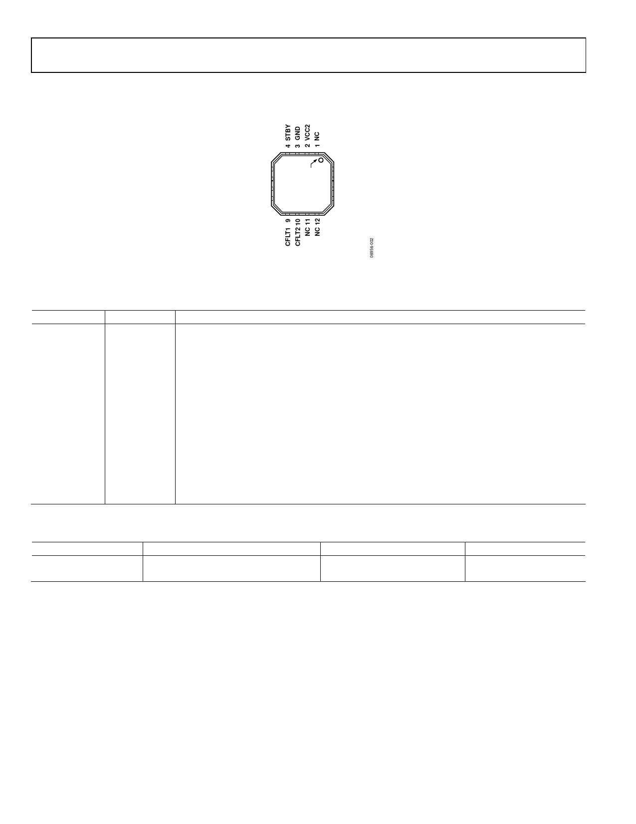
Figure 2. Pin Configuration
Table 4. Pin Function Descriptions
Pin No.
Mnemonic
Description
1, 11, 12, 13, 16 NC
No Connect. Do not connect these pins.
2
VCC2
This power supply pin should be connected to the supply via a choke circuit (see Figure 19).
3, 7
GND
Connected to Ground.
4
STBY
When STBY is low (0 V), the device operates in transmit mode. When the radio is receiving data, STBY
can be taken high (2.5 V), reducing the supply current to 9 mA.
5
VCC1
Connect to Power Supply.
6
RFIN
RF Input.
8
VREG
When VREG is low, the device goes into sleep mode, reducing the supply current to less than 1 μA.
When VREG is high (2.85 V), the device operates in its normal transmit mode. When high, VREG draws
a bias current of approximately 9 mA.
9, 10
CFLT1, CFLT2 Ground-Referenced Capacitors. These should be connected to reduce bias line noise.
14, 15
RFOUT
Unmatched RF Outputs. These parallel outputs are matched to 50 Ω using a microstrip line and shunt
capacitor. The power supply voltage should be connected to these pins through a choke inductor.
Exposed
Paddle
The exposed paddle should be soldered down to a low impedance ground plane (use multiple vias,
at least 9, to stitch together the ground planes) for optimum electrical and thermal performance.
Table 5. Operating Modes1
Mnemonic
Normal Operation
VREG
High
STBY
Low
1 X = don’t care.
Standby Mode
High
High
Sleep Mode
Low
X
Rev. 0 | Page 6 of 16
Share Link: 