ADL5570 データシートの表示(PDF) - Analog Devices
部品番号
コンポーネント説明
一致するリスト
ADL5570 Datasheet PDF : 12 Pages
| |||
ADL5570
EVALUATION BOARD
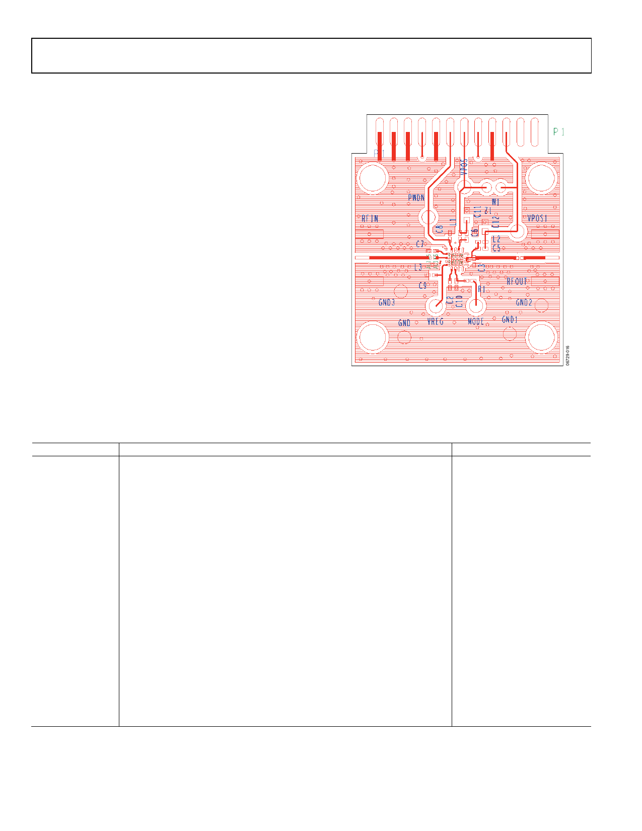
The evaluation board layout is shown in Figure 16. The ADL5570
performance data was taken on a FR4 board. During board
layout, 50 Ω RF trace impedance must be ensured. The output
matching capacitor, C3, is placed 30 mils from the package edge.
Figure 16. Evaluation Board Layout
Table 6. Evaluation Board Configuration Options
Component
Function
VPOS, VPOS1, GND Supply and Ground Connections.
TP1 (STBY)
Transmit/Standby Mode: When STBY is low (0 V), the device operates in transmit
mode. When the radio is receiving data, STBY can be taken high (2.5 V), reducing
the supply current to 10 mA.
TP2 (VREG)
Normal/Sleep Mode: When VREG is low, the device goes into sleep mode,
reducing the supply current to 10 μA. When VREG is high (2.85 V), the device
operates in its normal transmit mode. When high, VREG draws a bias current of
approximately 10 mA.
TP5 (MODE), R1
High/Low Power Mode: Switches between high power mode and low power
mode. When MODE is low (0 V), the device operates in high power mode.
When MODE is high (2.5 V), the device operates in low power mode.
L3
Input Interface: L3 matches the input to 50 Ω.
C3, C4
Output Interface: C4 provides dc blocking, and C3 matches the output to 50 Ω.
C2
C7 to C12
L1, L2, C6, C5
Filter Interface: A ground-referenced capacitor should be connected to this
node to reduce bias line noise.
Power Supply Decoupling: The capacitors, C7 through C12, are used for power
supply decoupling. They should be placed as close as possible to the DUT.
RF Trap: L1, C6 and L2, C5 form tank circuits and prevent RF from propagating
on the dc supply lines.
Default Value
W1 = Installed
Not applicable
Not applicable
R1 = 50 kΩ (Size 0402)
L3 = 2.7 nH (Size 0402)
C4 = 39 pF (Size 0402)
C3 = 3.3 pF (Size 0402)
(Tight tolerance recommended)
C2 = 2.2 pF (Size 0402)
C7 to C10 = 0.01 μF (Size 0402)
C11, C12 = 1 μF (Size 0402)
L1 = 1 nH (Size 0402)
C6 = 3.6 pF (Size 0402)
L2 = 11 nH (Size 0402)
C5 = Open
Rev. 0 | Page 10 of 12
Share Link: 