AD1984B データシートの表示(PDF) - Analog Devices
部品番号
コンポーネント説明
一致するリスト
AD1984B Datasheet PDF : 20 Pages
| |||
AD1984B
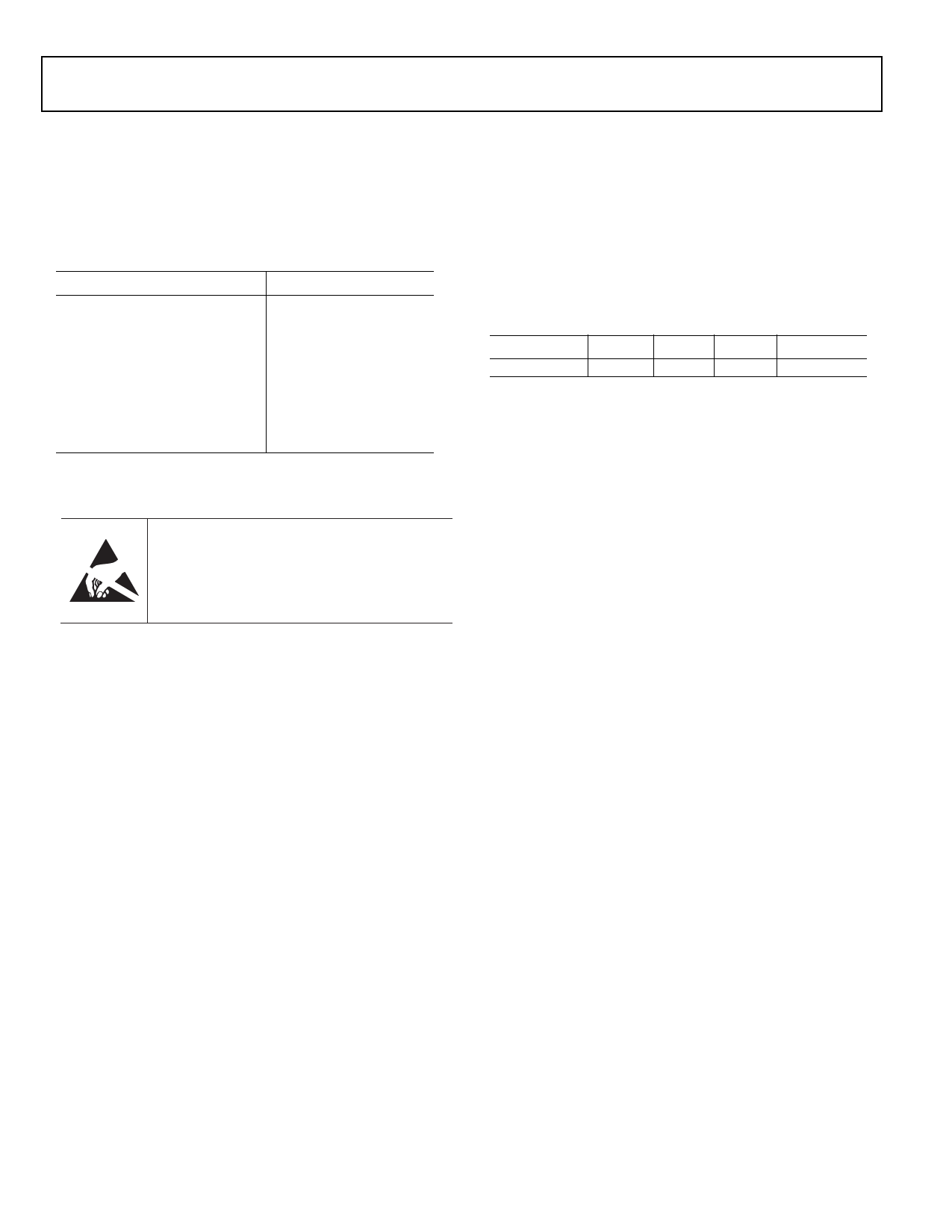
ABSOLUTE MAXIMUM RATINGS
Stresses greater than those listed below may cause permanent
damage to the device. This is a stress rating only; functional
operation of the device at these or any other conditions above
those indicated in the operational section of this specification is
not implied. Exposure to absolute maximum rating conditions
for extended periods may affect device reliability.
Parameter
Rating
Digital (DVDD)
Digital (DVCORE)
Digital I/O (DVIO)
Analog (AVDD)
Input Current (except supply pins)
Analog Input Voltage (Signal Pins)
Digital Input Voltage (Signal Pins)
Ambient Temperature (Operating)
Storage Temperature
–0.30 V to +3.65 V
–0.30 V to +2.10 V
–0.30 V to +3.65 V
–0.30 V to +3.65 V
±10.0 mA
–0.30 V to AVDD +0.3 V
–0.30 V to DVIO +0.3 V
0°C to +70°C
–65°C to +150°C
ESD CAUTION
ESD (electrostatic discharge) sensitive device.
Charged devices and circuit boards can discharge
without detection. Although this product features
patented or proprietary protection circuitry, damage
may occur on devices subjected to high energy ESD.
Therefore, proper ESD precautions should be taken to
avoid performance degradation or loss of functionality.
ENVIRONMENTAL CONDITIONS
Ambient Temperature Rating:
TAMB = TCASE – (PD × θCA)
TCASE = case temperature in °C
PD = power dissipation in W
θCA = thermal resistance (case-to-ambient)
θJA = thermal resistance (junction-to-ambient)
θJC = thermal resistance (junction-to-case)
All measurements per EIA-JESD51 with 2S2P test board per
EIA-JESD51-7.
Package
θJA
LFCSP_VQ
47
θJC
θCA
Unit
15
32
°C/W
Rev. 0 | Page 8 of 20 | February 2008
Share Link: 