ACT4088US-T8082 データシートの表示(PDF) - Active-Semi, Inc
部品番号
コンポーネント説明
一致するリスト
ACT4088US-T8082 Datasheet PDF : 12 Pages
| |||
ACT4088
Rev 2, 15-Nov-12
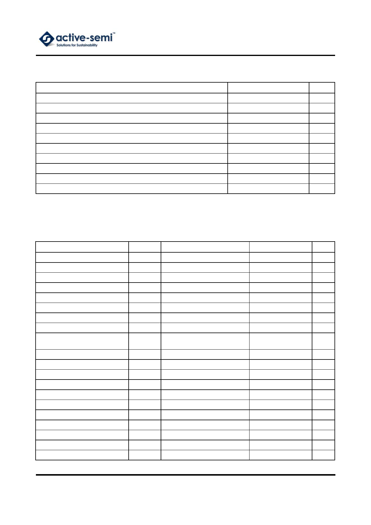
ABSOLUTE MAXIMUM RATINGSc
PARAMETER
IN Supply Voltage
SW Voltage
BST Voltage
EN, FB Voltage
Continuous SW Current
Junction to Ambient Thermal Resistance (θJA)
Maximum Power Dissipation
Operating Junction Temperature
Storage Temperature
Lead Temperature (Soldering, 10 sec)
VALUE
-0.3 to 32
-1 to VIN + 1
VSW - 0.3 to VSW + 7
-0.3 to 6
Internally Limited
220
0.5
-40 to 150
-55 to 150
300
UNIT
V
V
V
V
A
°C/W
W
°C
°C
°C
c: Do not exceed these limits to prevent damage to the device. Exposure to absolute maximum rating conditions for long periods may
affect device reliability.
ELECTRICAL CHARACTERISTICS
(VIN = 12V, TA = 25°C, unless otherwise specified.)
PARAMETER
Input Voltage
Under Voltage Lockout Voltage
Under Voltage Lockout Hysteresis
Feedback Voltage
Frequency Foldback Threshold
High-side Switch On Resistance
Low-side Switch On Resistance
SW Leakage
Current Limit
Switching Frequency
Foldback Switching Frequency
Maximum Duty Cycle
Minimum On-Time
EN Threshold Voltage
EN Hysteresis
EN Internal Pull-up Current
Supply Current in Shutdown
Supply Current in Operation
Thermal Shutdown Temperature
Thermal Shutdown Hysteresis
SYMBOL
TEST CONDITIONS
VIN
VUVLO
VOUT = 3.3V, ILOAD = 0A to 1.5A
Input Voltage Rising
VFB
4.75V ≤ VIN ≤ 20V, VCOMP = 1.5V
RONH
RONH
ILTM
fSW
DMAX
VEN = 0, VSW = 0V
VIN = 12V, VOUT = 5V, or
EN = G, SW = G
VFB = 0V, or FB = G
VFB = 0.6V
EN Rising
EN Rising
VEN = 0V or EN = G
VEN = 2V, VFB = 1.0V
MIN
4.5
4
0.79
TYP MAX
28
4.2 4.49
250
0.81 0.83
250
0.300
15
1
10
UNIT
V
V
mV
V
mV
Ω
Ω
µA
1.8
A
1.1 1.4 1.6 MHz
467
kHz
92
%
75
ns
1.12 1.24 1.36
V
100
mV
2
µA
15 30
µA
1
2
mA
160
°C
10
°C
Innovative PowerTM
-3-
www.active-semi.com
Copyright © 2012 Active-Semi, Inc.
Share Link: 