ACT4070B データシートの表示(PDF) - Active-Semi, Inc
部品番号
コンポーネント説明
一致するリスト
ACT4070B Datasheet PDF : 9 Pages
| |||
ORDERING INFORMATION
PART NUMBER
ACT4070BYH
ACT4070BYH-T
TEMPERATURE RANGE
-40°C to 85°C
-40°C to 85°C
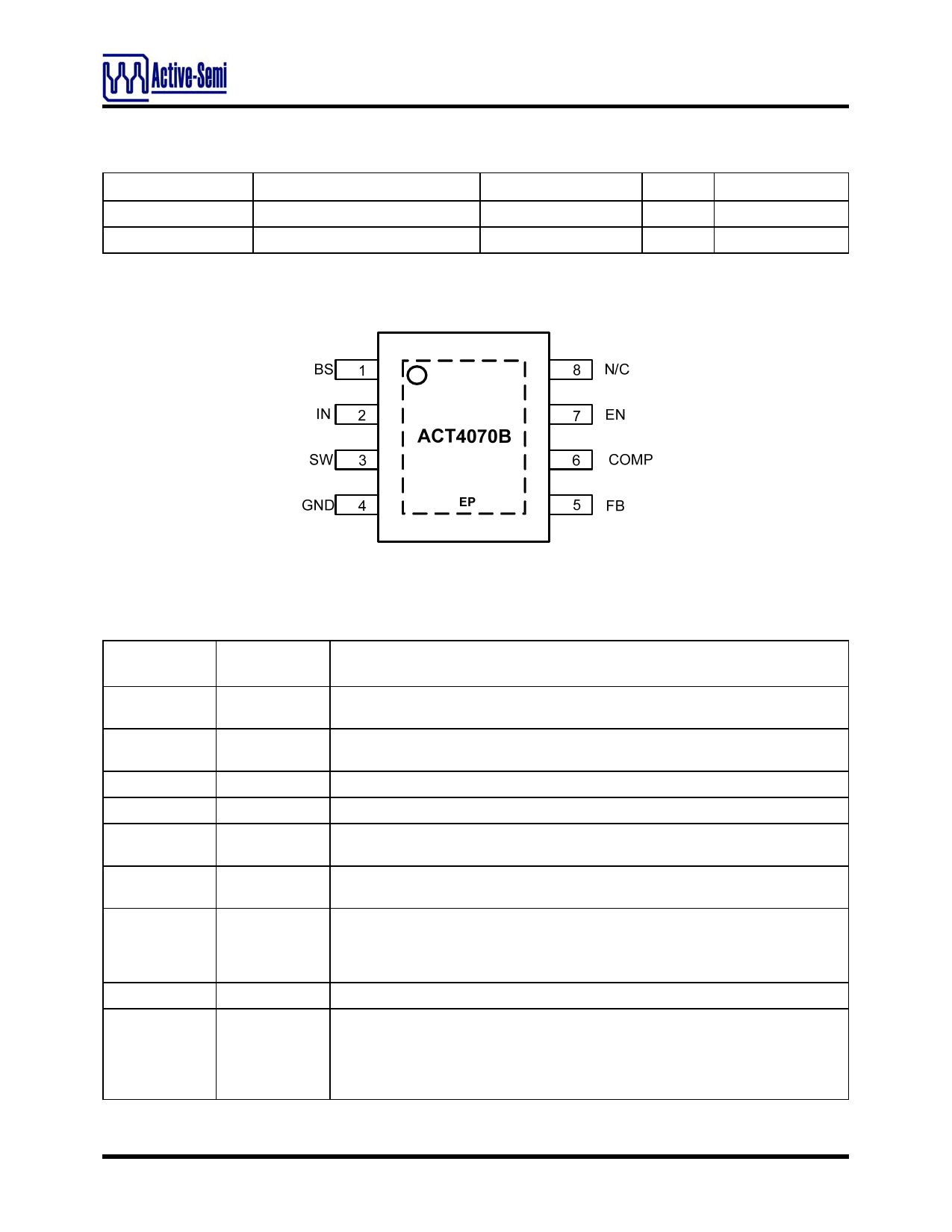
PIN CONFIGURATION
ACT4070B
Rev 0, 23-Apr-12
PACKAGE
SOP-8/EP
SOP-8/EP
PINS
8
8
PACKING
TUBE
TAPE & REEL
PIN DESCRIPTION
SOP-8/EP
PIN NUMBER PIN NAME
PIN DESCRIPTION
1
BS
Bootstrap. This pin acts as the positive rail for the high-side switch’s gate driver.
Connect a 10nF between this pin and SW.
2
IN
Input Supply. Bypass this pin to GND with a low ESR capacitor. See Input Ca-
pacitor in Application Information section.
3
SW
Switch Output. Connect this pin to the switching end of the inductor.
4
GND
Ground.
5
FB
Feedback Input. The voltage at this pin is regulated to 0.808V. Connect to the
resistor divider between output and ground to set output voltage.
6
COMP
Compensation Pin. See Compensation Technique in Application Information sec-
tion.
Enable Input. When higher than 1.6V, this pin turns the IC on. When lower than
7
EN
1.5V, this pin turns the IC off. This pin has a small internal pull up current to a high
level voltage when pin is not connected.
8
N/C
Not Connected.
Exposed Pad shown as dashed box. The exposed thermal pad should be con-
nected to board ground plane and pin 4. The ground plane should include a large
EP
EP
exposed copper pad under the package for thermal dissipation (see package out-
line). The leads and exposed pad should be flush with the board, without offset
from the board surface.
Innovative PowerTM
-2-
www.active-semi.com
Copyright © 2012 Active-Semi, Inc.
Share Link: 