ACS756KCA-050B-PFF-T データシートの表示(PDF) - Allegro MicroSystems
部品番号
コンポーネント説明
一致するリスト
ACS756KCA-050B-PFF-T
Allegro MicroSystems

ACS756KCA-050B-PFF-T Datasheet PDF : 11 Pages
| |||
ACS756
Fully Integrated, Hall Effect-Based Linear Current Sensor IC
with 3 kVRMS Voltage Isolation and a Low-Resistance Current Conductor
Features and Benefits
▪ Industry-leading noise performance through proprietary
amplifier and filter design techniques
▪ Total output error 0.8% at TA= 25°C
▪ Small package size, with easy mounting capability
▪ Monolithic Hall IC for high reliability
▪ Ultra-low power loss: 130 μΩ internal conductor resistance
▪ 3 kVRMS minimum isolation voltage from
pins 1-3 to pins 4-5
▪ 3.0 to 5.0 V, single supply operation
▪ 3 μs output rise time in response to step input current
▪ 20 or 40 mV/A output sensitivity
▪ Output voltage proportional to AC or DC currents
▪ Factory-trimmed for accuracy
▪ Extremely stable output offset voltage
▪ Nearly zero magnetic hysteresis
TÜV America
Certificate Number:
U8V 09 05 54214 021
Package: 5 pin package (suffix PFF)
1
Additional leadforms available for qualifying volumes
Description
The Allegro ACS756 family of current sensor ICs provides
economical and precise solutions for AC or DC current sensing
in industrial, automotive, commercial, and communications
systems. The device package allows for easy implementation by
the customer. Typical applications include motor control, load
detection and management, power supplies, and overcurrent
fault protection.
The device consists of a precision, low-offset linear Hall
circuit with a copper conduction path located near the die.
Applied current flowing through this copper conduction path
generates a magnetic field which the Hall IC converts into a
proportional voltage. Device accuracy is optimized through the
close proximity of the magnetic signal to the Hall transducer.
A precise, proportional voltage is provided by the low-offset,
chopper-stabilized BiCMOS Hall IC, which is programmed
for accuracy at the factory.
The output of the device has a positive slope (>VCC / 2) when an
increasing current flows through the primary copper conduction
path (from terminal 4 to terminal 5), which is the path used
for current sampling. The internal resistance of this conductive
path is 130 μΩ typical, providing low power loss.
The thickness of the copper conductor allows survival of the
device at up to 5× overcurrent conditions. The terminals of the
Continued on the next page…
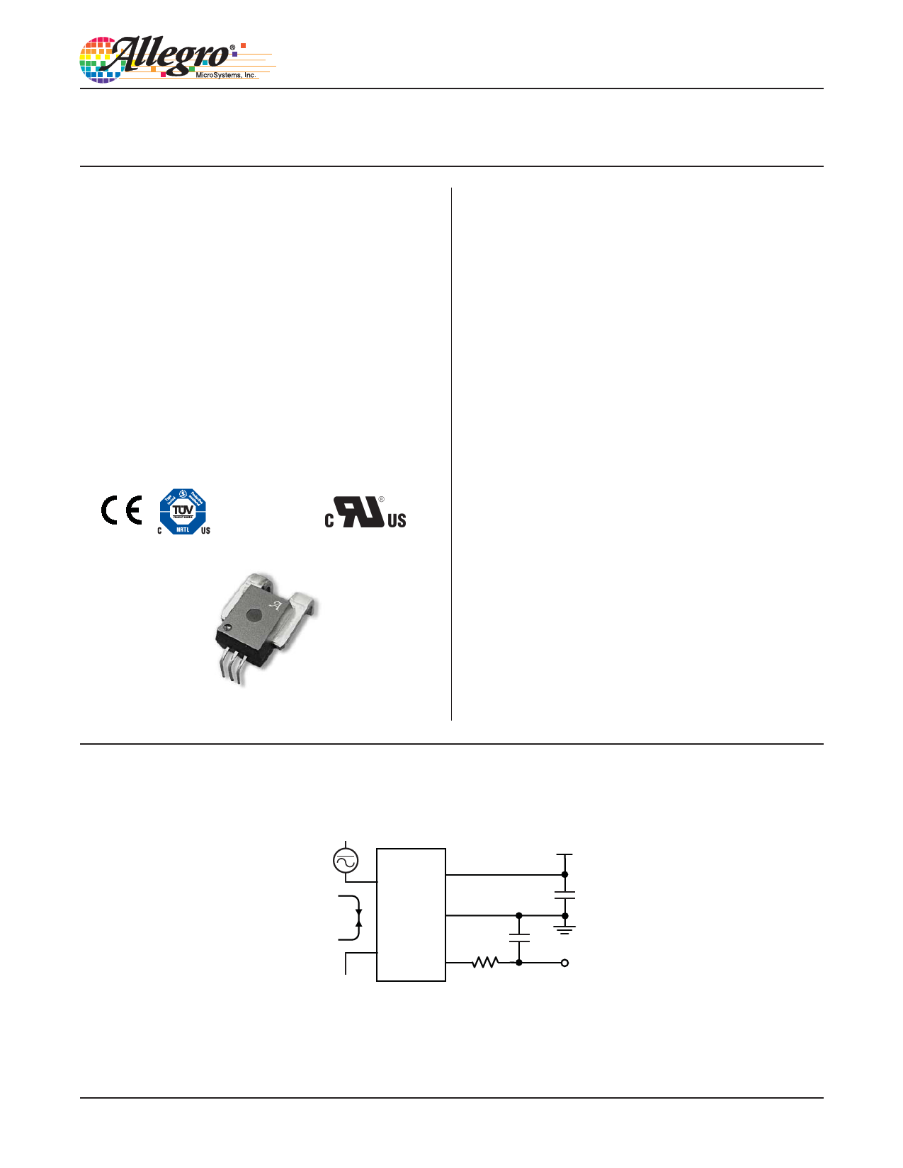
Typical Application
ACS756-DS, Rev. 6
4
IP+
1
VCC
ACS756
IP
GND 2
5
IP–
3
VIOUT
+5 V
CBYP
0.1 μF
CF
RF
VOUT
Application 1. The ACS756 outputs an analog signal, VOUT , that
varies linearly with the uni- or bi-directional AC or DC primary
sampled current, IP , within the range specified. CF is for optimal
noise management, with values that depend on the application.
Share Link: