7C185-20 データシートの表示(PDF) - Cypress Semiconductor
部品番号
コンポーネント説明
一致するリスト
7C185-20 Datasheet PDF : 11 Pages
| |||
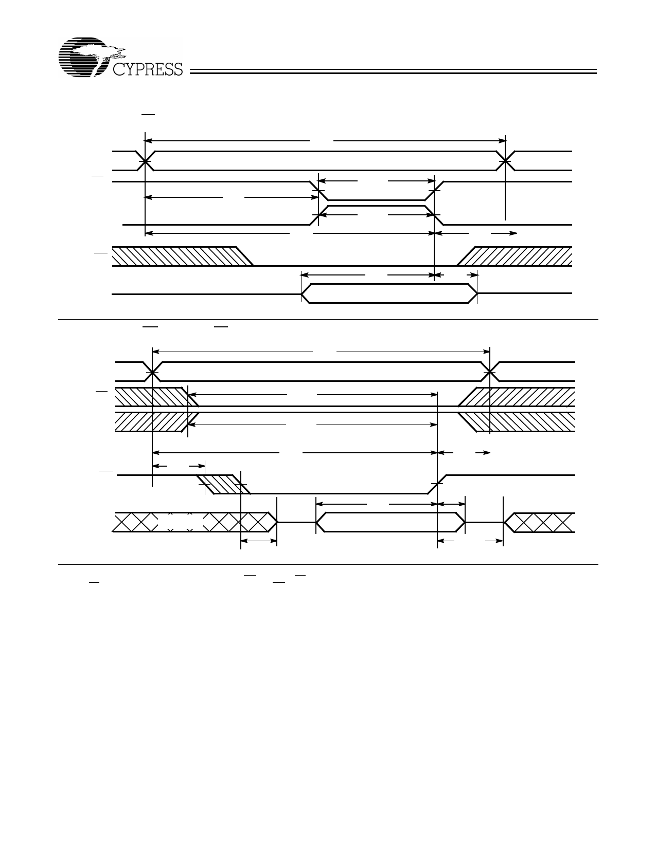
Switching Waveforms (continued)
rite Cycle No. 2 (CE Controlled)[13,14,15]
ADDRESS
CE1
tSA
CE2
WE
DATA I/O
tWC
tSCE1
tSCE2
tAW
tHA
tSD
tHD
DATA IN VALID
Write Cycle No. 3 (WE Controlled, OE LOW)[13,14,15,16]
tWC
ADDRESS
CE1
tSCE1
CE2
tSCE2
tAW
tHA
tSA
WE
DATA I/O
NOTE 14
tHZWE
tSD
DATA IN VALID
tHD
tLZWE
Notes:
15. The minimum write cycle time for write cycle #3 (WE controlled, OE LOW) is the sum of tHZWE and tSD.
16. If CE1 goes HIGH or CE2 goes LOW simultaneously with WE HIGH, the output remains in a high-impedance state.
CY7C185
Document #: 38-05043 Rev. *A
Page 6 of 11
Share Link: 