74AHC1G86-Q100 データシートの表示(PDF) - NXP Semiconductors.
部品番号
コンポーネント説明
一致するリスト
74AHC1G86-Q100 Datasheet PDF : 13 Pages
| |||
NXP Semiconductors
74AHC1G86-Q100; 74AHCT1G86-Q100
2-input EXCLUSIVE-OR gate
Table 8. Dynamic characteristics …continued
GND = 0 V; tr = tf = 3.0 ns. For waveform see Figure 5. For test circuit see Figure 6.
Symbol Parameter Conditions
25 C
40 C to +85 C 40 C to +125 C Unit
Min Typ Max Min Max
Min
Max
For type 74AHCT1G86-Q100
tpd
propagation A and B to Y
[1]
delay
VCC = 4.5 V to 5.5 V
[3]
CL = 15 pF
- 3.5 6.9 1.0
8.0
1.0
9.0 ns
CL = 50 pF
- 5.0 7.9 1.0
9.0
1.0
10.5 ns
CPD
power
per buffer;
[4] -
11
-
-
-
-
-
pF
dissipation CL = 50 pF; f = 1 MHz;
capacitance VI = GND to VCC
[1] tpd is the same as tPLH and tPHL.
[2] Typical values are measured at VCC = 3.3 V.
[3] Typical values are measured at VCC = 5.0 V.
[4] CPD is used to determine the dynamic power dissipation PD (W).
PD = CPD VCC2 fi + (CL VCC2 fo) where:
fi = input frequency in MHz;
fo = output frequency in MHz;
CL = output load capacitance in pF;
VCC = supply voltage in Volts.
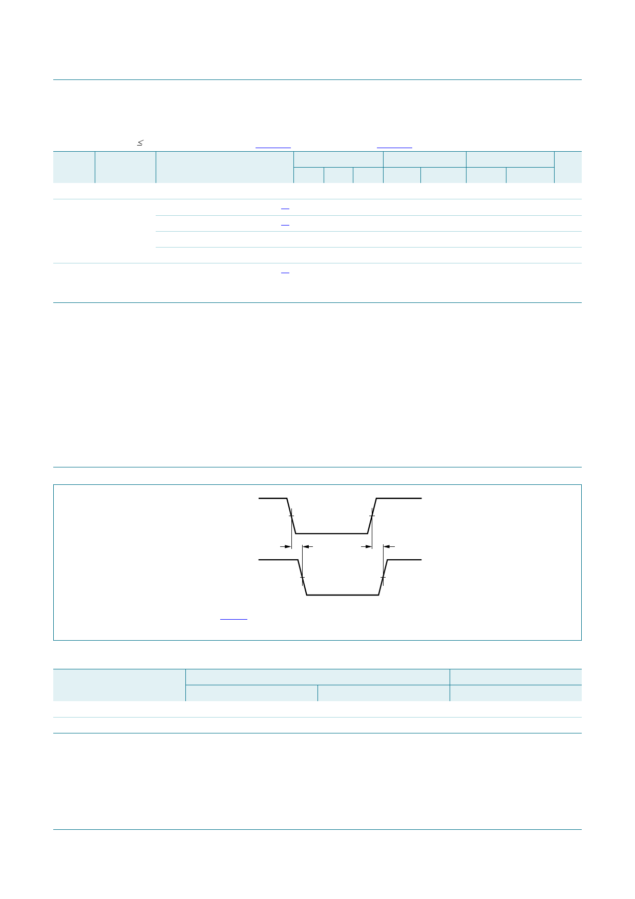
12. Waveforms
A, B input
Y output
VM
tPHL
VM
Measurement points are given in Table 9.
Fig 5. The input (A and B) to output (Y) propagation delays
Table 9. Measurement points
Type
Input
74AHC1G86-Q100
74AHCT1G86-Q100
VI
GND to VCC
GND to 3.0 V
VM
0.5 VCC
1.5 V
tPLH
mna041
Output
VM
0.5 VCC
0.5 VCC
74AHC_AHCT1G86_Q100
Product data sheet
All information provided in this document is subject to legal disclaimers.
Rev. 1 — 16 July 2012
© NXP B.V. 2012. All rights reserved.
6 of 13
Share Link: 