MAX662A データシートの表示(PDF) - Maxim Integrated
部品番号
コンポーネント説明
一致するリスト
MAX662A Datasheet PDF : 6 Pages
| |||
+12V, 30mA Flash Memory
Programming Supply
_______________Detailed Description
Operating Principle
The MAX662A provides a regulated 12V output voltage
at 30mA from a 5V ±5% power supply, making it ideal
for flash EEPROM programming applications. It uses
internal charge pumps and external capacitors to gen-
erate +12V, eliminating inductors. Regulation is provid-
ed by a pulse-skipping scheme that monitors the
output voltage level and turns on the charge pumps
when the output voltage begins to droop.
Figure 1 shows a simplified block diagram of the
MAX662A. When the S1 switches are closed and the
S2 switches are open, capacitors C1 and C2 are
charged up to VCC. The S1 switches are then opened
and the S2 switches are closed so that capacitors C1
and C2 are connected in series between VCC and
VOUT. This performs a voltage tripling function. A pulse-
skipping feedback scheme adjusts the output voltage
to 12V ±5%. The efficiency of the MAX662A with VCC =
5V and IOUT = 30mA is typically 76%. See the
Efficiency vs. Load Current graph in the Typical
Operating Characteristics.
During one oscillator cycle, energy is transferred from
the charge-pump capacitors to the output filter capaci-
tor and the load. The number of cycles within a given
time frame increases as the load current increases or
as the input supply voltage decreases. In the limiting
case, the charge pumps operate continuously, and the
oscillator frequency is nominally 500kHz.
5V
0V
12V
5V
200µs/div
CIRCUIT OF FIGURE 3, VCC = 5V, IOUT = 200µA
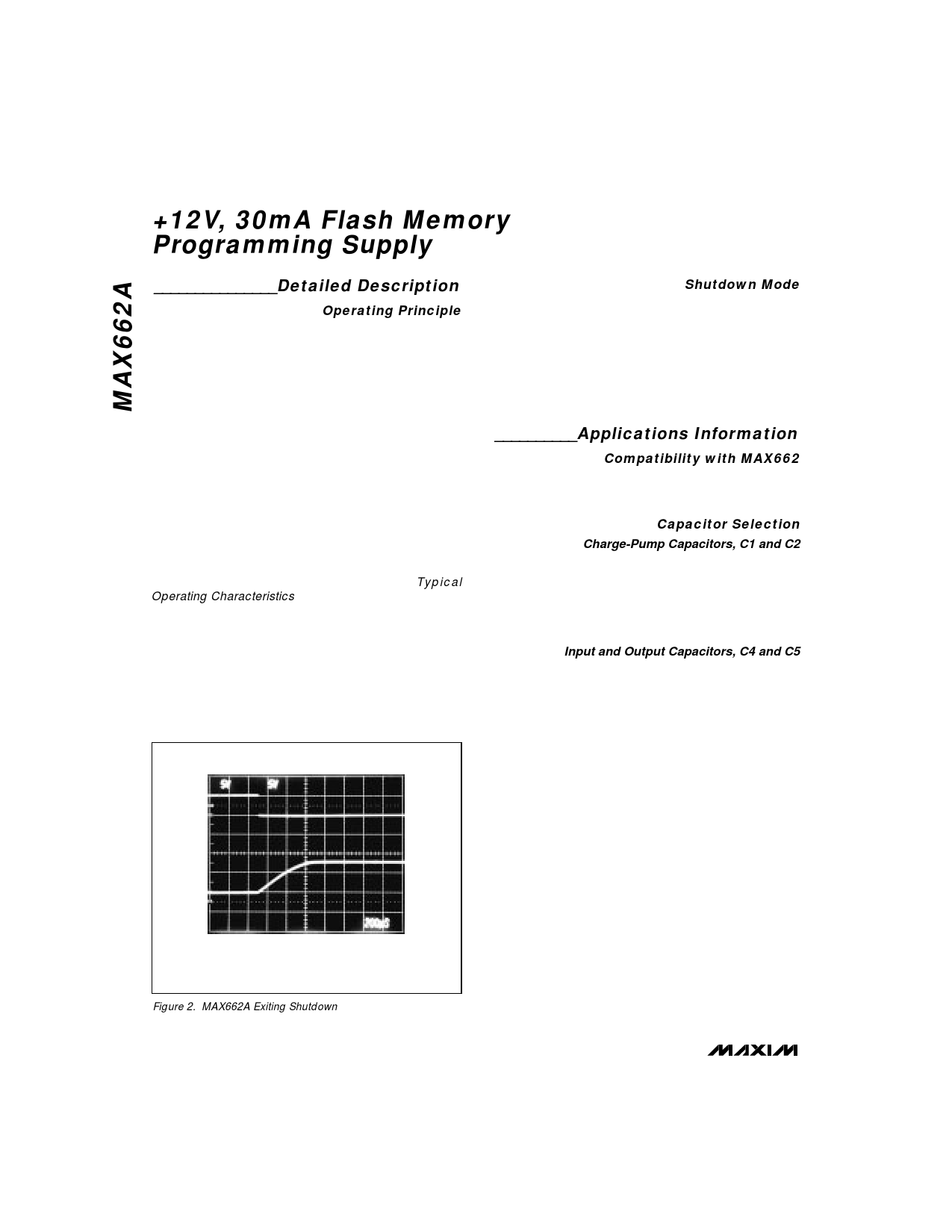
Figure 2. MAX662A Exiting Shutdown
SHDN
VOUT
Shutdown Mode
The MAX662A enters shutdown mode when SHDN is a
logic high. SHDN is a TTL/CMOS-compatible input sig-
nal that is internally pulled up to VCC. In shutdown
mode, the charge-pump switching action is halted and
VIN is connected to VOUT through a 1kΩ switch. When
entering shutdown, VOUT declines to VCC in typically
13ms. Connect SHDN to ground for normal operation.
When VCC = 5V, it takes typically 400µs for the output
to reach 12V after SHDN goes low (Figure 2).
__________Applications Information
Compatibility with MAX662
The MAX662A is a 100%-compatible upgrade of the
MAX662. The MAX662A does not require capacitor C3,
although its presence does not affect performance.
Capacitor Selection
Charge-Pump Capacitors, C1 and C2
The capacitance values of the charge-pump capacitors
C1 and C2 are critical. Use ceramic or tantalum capaci-
tors in the 0.22µF to 1.0µF range. For applications requir-
ing operation over extended and/or military temperature
ranges, use 1.0µF tantalum capacitors for C1 and C2
(Figure 3b).
Input and Output Capacitors, C4 and C5
The type of input bypass capacitor (C4) and output filter
capacitor (C5) affects performance. Tantalums, ceramics
or aluminum electrolytics are suggested. For smallest size,
use Sprague 595D475X9016A7 surface-mount capacitors,
which are 3.51mm x 1.81mm. For lowest ripple, use low-
ESR through-hole ceramic or tantalum capacitors. For low-
est cost, use aluminum electrolytic or tantalum capacitors.
Figure 3a shows the component values for proper opera-
tion over the commercial temperature range using mini-
mum board space. The input bypass capacitor (C4) and
output filter capacitor (C5) should both be at least 4.7µF
when using Sprague’s miniature 595D series of tantalum
chip capacitors. Figure 3b shows the suggested compo-
nent values for applications over extended and/or mili-
tary temperature ranges.
The values of C4 and C5 can be reduced to 2µF and
1µF, respectively, when using ceramic capacitors. If
using aluminum electrolytics, choose capacitance values
of 10µF or larger for C4 and C5. Note that as VCC
increases above 5V and the output current decreases,
the amount of ripple at VOUT increases due to the slower
oscillator frequency combined with the higher input volt-
age. Increase the input and output bypass capacitance
to reduce output ripple.
Table 1 lists various capacitor suppliers.
4 _______________________________________________________________________________________
Share Link: 