WDD20-03S1(2010) データシートの表示(PDF) - CHINFA ELECTRONICS
部品番号
コンポーネント説明
一致するリスト
WDD20-03S1 Datasheet PDF : 4 Pages
| |||
PHYSICAL CHARACTERISTICS
Case size
Case material
Weight
Patting material
50.8 x 40.64 x 10.16 mm (2 x 1.6 x 0.4 inches)
Plastic base / Metal case
60 g
Epoxy
WDD20 SERIES
SINGLE & DUAL OUTPUT
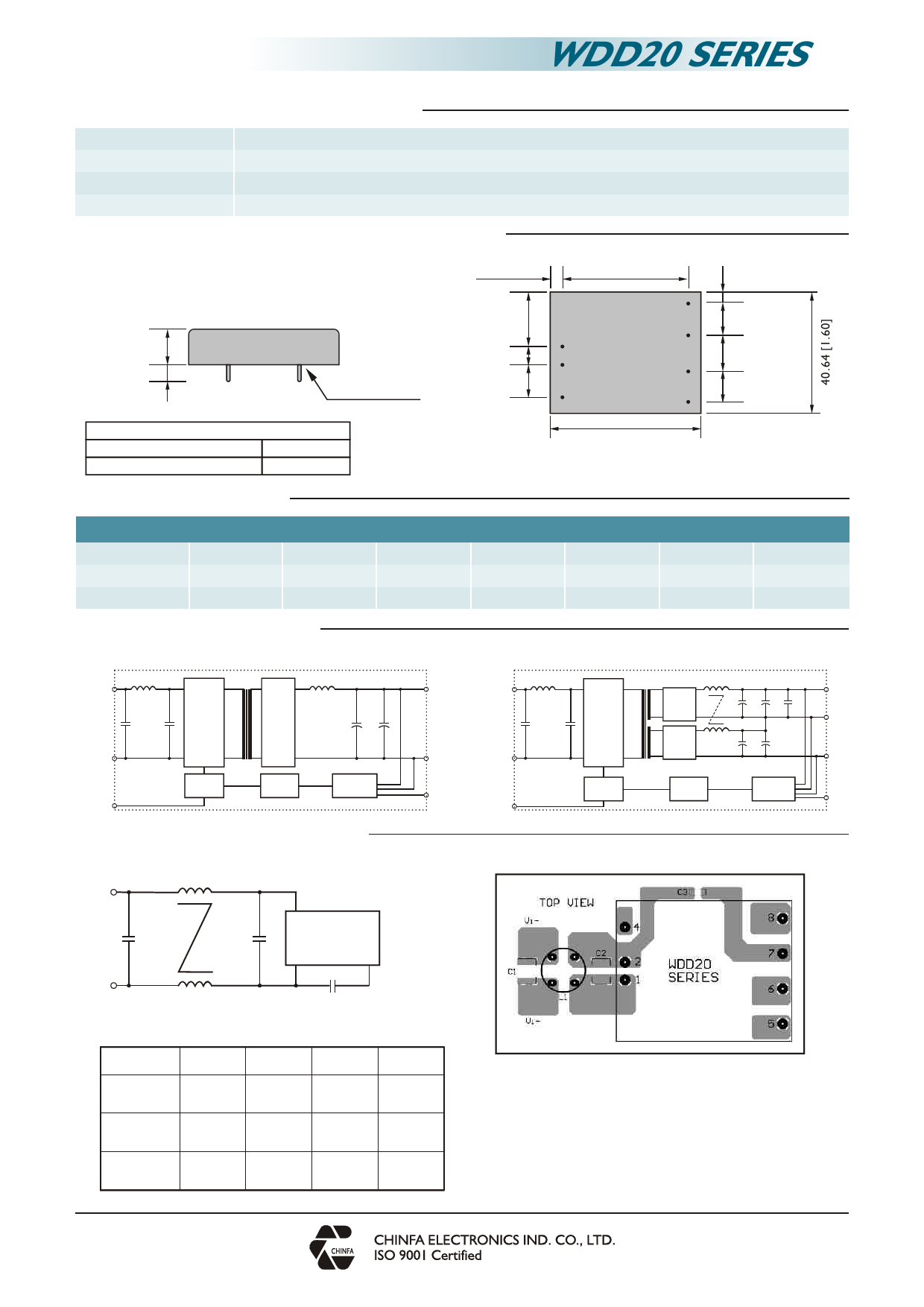
MECHANISM & PIN CONFIGURATION
mm [inch]
2.54 [0.10]
45.72 [1.80]
5.08 [0.20]
10.16 [0.4]
6.00 [0.24]
17.78 [0.70]
1
5.08 [0.20]
2
10.16 [0.40]
DIA 1.00 [0.04]
4
5
10.16 [0.40]
6
10.16 [0.40]
7
10.16 [0.40]
8
GENERAL TOLERANCE
0.00[0.00] - 30.00[1.18]
±0.30[0.01]
30.00[1.18] - 120.00[4.72]
±0.50[0.02]
50.80 [2.00]
BOTTOM VIEW
PIN ASSIGNMENT
GENERAL
PIN NO.
1
SINGLE
Vi+
DUAL
Vi+
2
4
5
6
7
8
Vi -
ON / OFF
NO PIN
Vo +
Vo -
Trim
Vi -
ON / OFF
Vo +
com
Vo -
Trim
CIRCUIT SCHEMATIC
‧Block diagram for WDD20 series with single output
‧Block diagram for WDD20 series with dual output
Vi +
Switching
Device
Rectifier
Vo +
Vi -
ON / OFF
Vo -
PWM
Opto -
Reference &
Controller
Isolation
Error Amp.
Trim
RECOMMENDED CIRCUIT
‧Recommended filter for EN55022 Class B compliance
L1
+
Vin +
Vo +
C1
C2
WDD20
Vin -
Vo -
-
C3
‧The commponents used in the above figure, together with the
manufacturer part numbers for these components, are as follows.
C1
C2
C3
3.3μF / 50V 3.3μF / 50V
WDD20-XXX1
MLCC
MLCC
InF / 2KV
MLCC
1μF / 50V
WDD20-XXX2
MLCC
1μF / 50V
MLCC
InF / 2KV
MLCC
3.3μF / 100V 3.3μF / 100V InF / 2KV
WDD20-XXX3
MLCC
MLCC
MLCC
L1
1.5mH
Common
Choke
1.5mH
Common
Choke
3.5mH
Common
Choke
www.chinfa.com
2010.02.09
Vi +
Vi -
ON / OFF
Switching
Device
PWM
Controller
Rectifier
Rectifier
Opto -
Isolation
Reference &
Error Amp.
Vo +
com
Vo -
Trim
‧Recommended EN 55022 Class B filter circuit layout.
sales@chinfa.com
P3
Share Link: 