P4C148-10PC データシートの表示(PDF) - Performance Semiconductor
部品番号
コンポーネント説明
一致するリスト
P4C148-10PC Datasheet PDF : 6 Pages
| |||
P4C148/P4C149
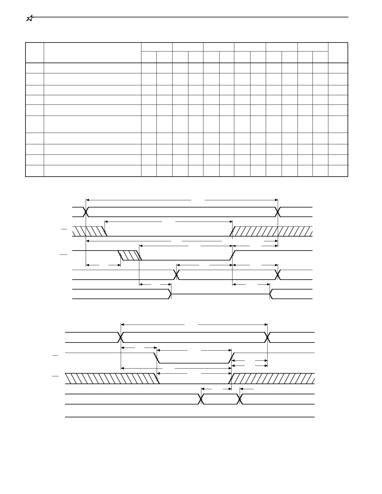
AC CHARACTERISTICS—WRITE CYCLE
(VCC = 5V ± 10%, All Temperature Ranges)(2)
Sym.
Parameter
-10
-12
-15
-20
-25
-35
Min Max Min Max Min Max Min Max Min Max Min Max Unit
tWC Write Cycle Time
10
12
15
20
25
35
ns
tCW Chip Enable Time to End of Write 8
10
12
16
20
25
ns
t Address Valid to End of Write
8
10
12
16
20
25
ns
AW
tAS Address Set-up Time
0
0
0
0
0
0
ns
tWP Write Pulse Width
8
10
12
16
20
25
ns
t Address Hold Time from
AH End of Write
0
0
0
0
0
0
ns
tDW Data Valid to End of Write
5
6
7
9
12
16
ns
tDH Data Hold Time
0
0
0
0
0
0
ns
tWZ Write Enable to Output in High Z
5
6
7
7
8
12 ns
tOW Output Active from End of Write 0
0
0
0
0
0
ns
TIMING WAVEFORM OF WRITE CYCLE NO. 1 (WE CONTROLLED)(9)
(11)
t WC
ADDRESS
CE
t CW
t AW
t WP
t WR
t AH
WE
t AS
t DW
t DH
DATA IN
DATA OUT
DATA UNDEFINED
t
(12)
WZ
DATA VALID
t
(10,
OW
12)
HIGH IMPEDANCE
TIMING WAVEFORM OF WRITE CYCLE NO. 2 (CE/CS CONTROLLED)(9)
(11)
t WC
ADDRESS
CE
WE
DATA IN
t AS
t CW
t AW
t WP
t AH
t WR
t DW
t DH
DATA VALID
DATA OUT
HIGH IMPEDANCE
Notes:
9. CE and WE must be LOW for WRITE cycle.
10. If CE goes HIGH simultaneously with WE high, the output remains
in a high impedance state.
11. Write Cycle Time is measured from the last valid address to the first
transition address.
12. Transition is measured ±200mV from steady state voltage prior to
change with specified loading in Figure 1. This parameter is
sampled and not 100% tested.
22
Share Link: 