AD8346 データシートの表示(PDF) - Analog Devices
部品番号
コンポーネント説明
一致するリスト
AD8346 Datasheet PDF : 20 Pages
| |||
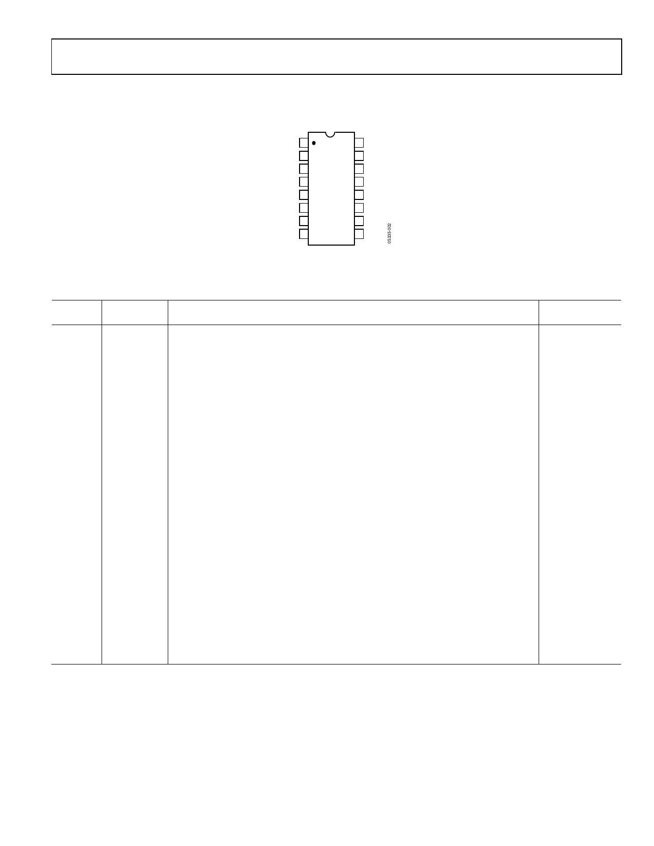
PIN CONFIGURATION AND FUNCTION DESCRIPTIONS
AD8346
IBBP 1
16 QBBP
IBBN 2
15 QBBN
COM1 3
14 COM4
COM1 4 AD8346 13 COM4
TOP VIEW
LOIN 5 (Not to Scale) 12 VPS2
LOIP 6
11 VOUT
VPS1 7
10 COM3
ENBL 8
9 COM2
Figure 2. Pin Configuration
Table 3. Pin Function Descriptions
Pin No.
1
2
3
4
5
6
7
8
9
10
11
12
13
14
15
16
Mnemonic
IBBP
IBBN
COM1
COM1
LOIN
LOIP
VPS1
ENBL
COM2
COM3
VOUT
VPS2
COM4
COM4
QBBN
QBBP
Description
I Channel Baseband Positive Input Pin. Input should be dc-biased to approximately 1.2 V.
Nominal characterized ac swing is 1 V p-p (0.7 V to 1.7 V). This makes the differential input
2 V p-p when IBBN is 180 degrees out of phase from IBBP.
I Channel Baseband Negative Input Pin. Input should be dc-biased to approximately 1.2 V.
Nominal characterized ac swing is 1 V p-p (0.7 V to 1.7 V). This makes the differential input
2 V p-p when IBBN is 180 degrees out of phase from IBBP.
Ground Pin for the LO phase splitter and LO buffers.
Ground Pin for the LO phase splitter and LO buffers.
LO Negative Input Pin. Internal dc bias (approximately VPS1 to 800 mV) is supplied. This
pin must be ac coupled.
LO Positive Input Pin. Internal dc bias (approximately VPS1 to 800 mV) is supplied. This pin
must be ac-coupled.
Power Supply Pin for the bias cell and LO buffers. This pin should be decoupled using
local 100 pF and 0.01 μF capacitors.
Enable Pin. A high level enables the device; a low level puts the device in sleep mode.
Ground Pin for the input stage of output amplifier.
Ground Pin for the output stage of output amplifier.
50 Ω DC-Coupled RF Output. User must provide ac coupling on this pin.
Power Supply Pin for baseband input voltage to current converters and mixer core. This
pin should be decoupled using local 100 pF and 0.01 μF capacitors.
Ground Pin for baseband input voltage to current converters and mixer core.
Ground Pin for baseband input voltage to current converters and mixer core.
Q Channel Baseband Negative Input. Input should be dc biased to approximately 1.2 V.
Nominal characterized ac swing is 1 V p-p. This makes the differential input 2 V p-p when
QBBN is 180° out of phase from QBBP.
Q Channel Baseband Positive Input. Input should be dc-biased to approximately 1.2 V.
Nominal characterized ac swing is 1 V p-p. This makes the differential input 2 V p-p when
QBBN is 180° out of phase from QBBP.
Equivalent
Circuit
Circuit A
Circuit A
Circuit B
Circuit B
Circuit C
Circuit D
Circuit A
Circuit A
Rev. A | Page 5 of 20
Share Link: 