MC74VHC1G03DFT1G データシートの表示(PDF) - ON Semiconductor
部品番号
コンポーネント説明
一致するリスト
MC74VHC1G03DFT1G Datasheet PDF : 6 Pages
| |||
MC74VHC1G03
Single 2−Input NOR Gate
with Open Drain Output
The MC74VHC1G03 is an advanced high speed CMOS 2−input
NOR gate with an open drain output fabricated with silicon gate
CMOS technology.
The internal circuit is composed of multiple stages, including an
open drain output which provides the capability to set output
switching level. This allows the MC74VHC1G03 to be used to
interface 5 V circuits to circuits of any voltage between VCC and 7 V
using an external resistor and power supply.
The MC74VHC1G03 input structure provides protection when
voltages up to 7 V are applied, regardless of the supply voltage.
Features
• High Speed: tPD = 3.6 ns (Typ) at VCC = 5 V
• Low Internal Power Dissipation: ICC = 1 mA (Max) at TA = 25°C
• Power Down Protection Provided on Inputs
• Pin and Function Compatible with Other Standard Logic Families
• Chip Complexity: FETs = 62
• Pb−Free Packages are Available
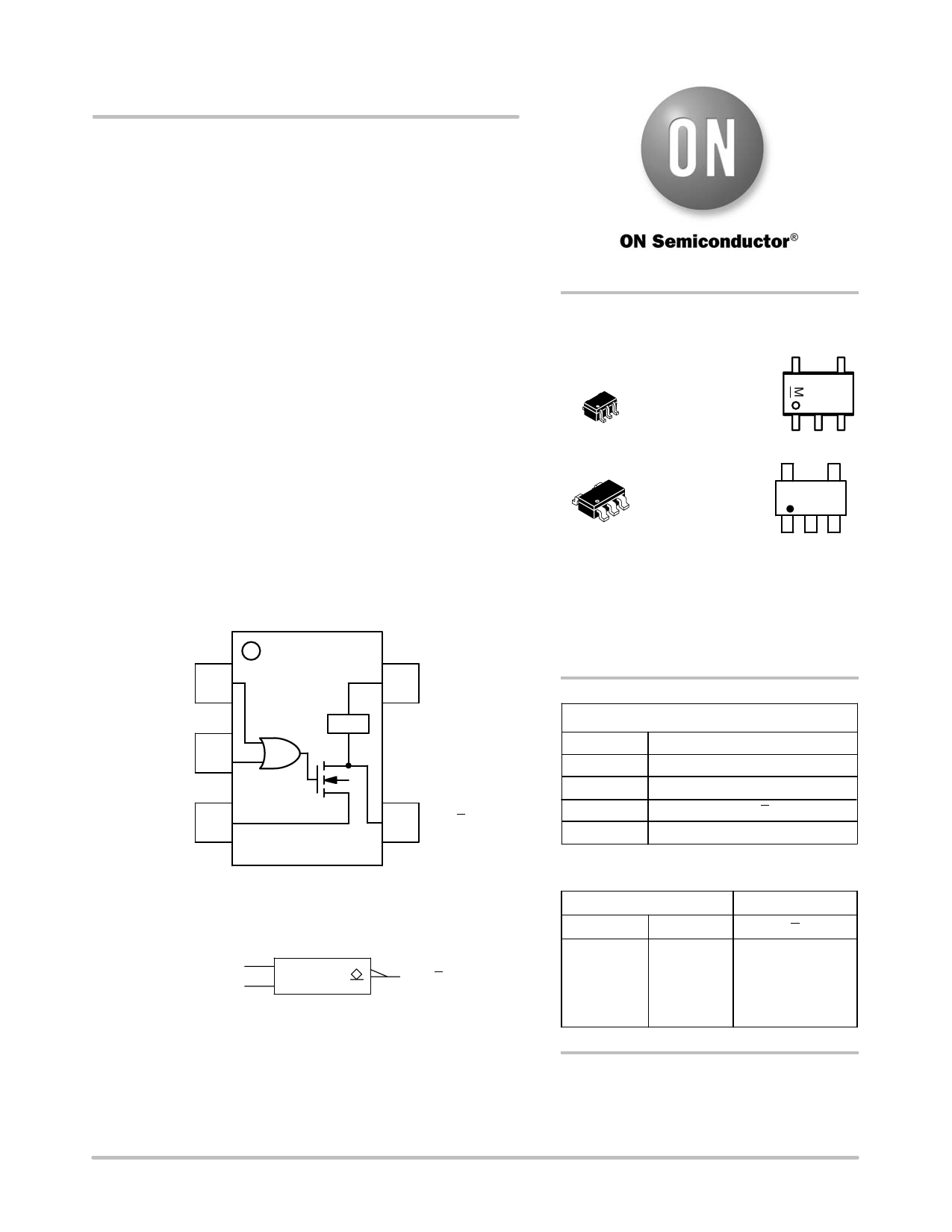
IN B 1
IN A 2
OVT
5 VCC
GND 3
4 OUT Y
Figure 1. Pinout (Top View)
IN A
≥1
IN B
OUT Y
Figure 2. Logic Symbol
http://onsemi.com
MARKING
DIAGRAMS
5
SC−88A / SOT−353 / SC−70
DF SUFFIX
CASE 419A
1
VP M G
G
TSOP−5 / SOT−23 / SC−59
DT SUFFIX
CASE 483
VP M G
G
VP = Device Code
M = Date Code*
G = Pb−Free Package
(Note: Microdot may be in either location)
*Date Code orientation and/or position may
vary depending upon manufacturing location.
PIN ASSIGNMENT
1
IN B
2
IN A
3
GND
4
OUT Y
5
VCC
FUNCTION TABLE
Inputs
A
B
L
L
L
H
H
L
H
H
Output
Y
Z
L
L
L
ORDERING INFORMATION
See detailed ordering and shipping information in the package
dimensions section on page 4 of this data sheet.
© Semiconductor Components Industries, LLC, 2007
1
January, 2007 − Rev. 14
Publication Order Number:
MC74VHC1G03/D
Share Link: 