MC10E163FNR2G データシートの表示(PDF) - ON Semiconductor
部品番号
コンポーネント説明
一致するリスト
MC10E163FNR2G Datasheet PDF : 8 Pages
| |||
MC10E163, MC100E163
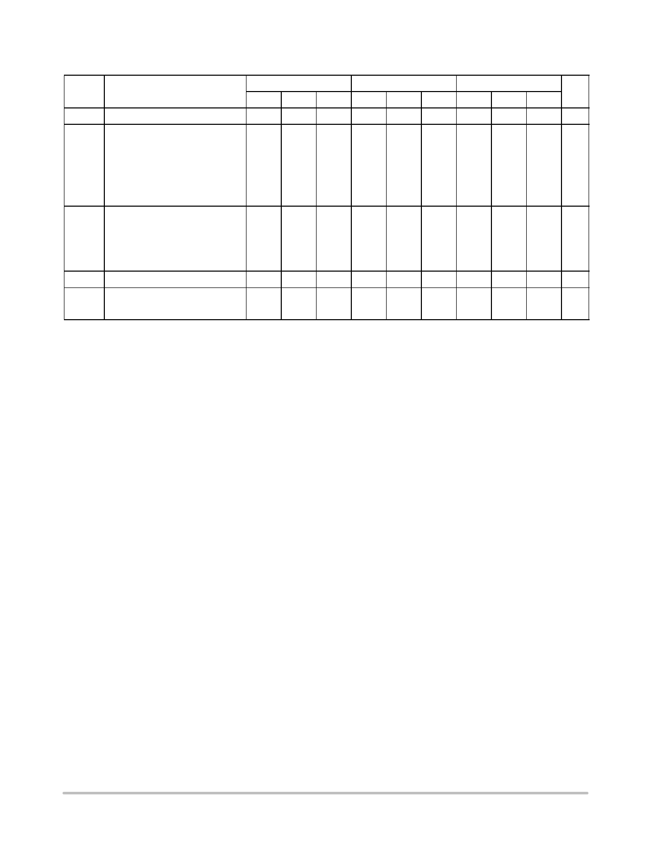
Table 8. AC CHARACTERISTICS VCCx = 5.0 V; VEE = 0.0 V or VCCx = 0.0 V; VEE = −5.0 V (Note 9)
0°C
25°C
85°C
Symbol
Characteristic
Min Typ Max Min Typ Max Min Typ Max Unit
fMAX
tPLH
tPHL
Maximum Toggle Frequency
700 1100
700 1100
700 1100
MHz
Propagation Delay to Output
ps
D 500 700 900 500 700 900 500 700 900
SEL0 500 765 1050 500 765 1050 500 765 1050
SEL1 525 735 950 525 735 950 525 735 950
SEL2 450 625 825 450 625 825 450 625 825
tSKEW Within-Device Skew (Note 10)
ps
An, Bn to Q
40
40
40
An, Am to QA
30
30
30
Bn, Bm to QB
30
30
30
tJITTER Random Clock Jitter (RMS)
<1
<1
<1
ps
tr
Rise/Fall Time
ps
tf
(20 - 80%)
275 375 575 275 375 575 275 375 575
NOTE: Device will meet the specifications after thermal equilibrium has been established when mounted in a test socket or printed circuit
board with maintained transverse airflow greater than 500 lfpm. Electrical parameters are guaranteed only over the declared
operating temperature range. Functional operation of the device exceeding these conditions is not implied. Device specification limit
values are applied individually under normal operating conditions and not valid simultaneously.
9. 10 Series: VEE can vary −0.46 V / +0.06 V.
100 Series: VEE can vary −0.46 V / +0.8 V.
10. Within-device skew is defined as identical transitions on similar paths through a device; n = 0-7, m n, m = 0-7.
http://onsemi.com
5
Share Link: 