MC10EL34DR2 データシートの表示(PDF) - ON Semiconductor
部品番号
コンポーネント説明
一致するリスト
MC10EL34DR2 Datasheet PDF : 8 Pages
| |||
MC10EL34, MC100EL34
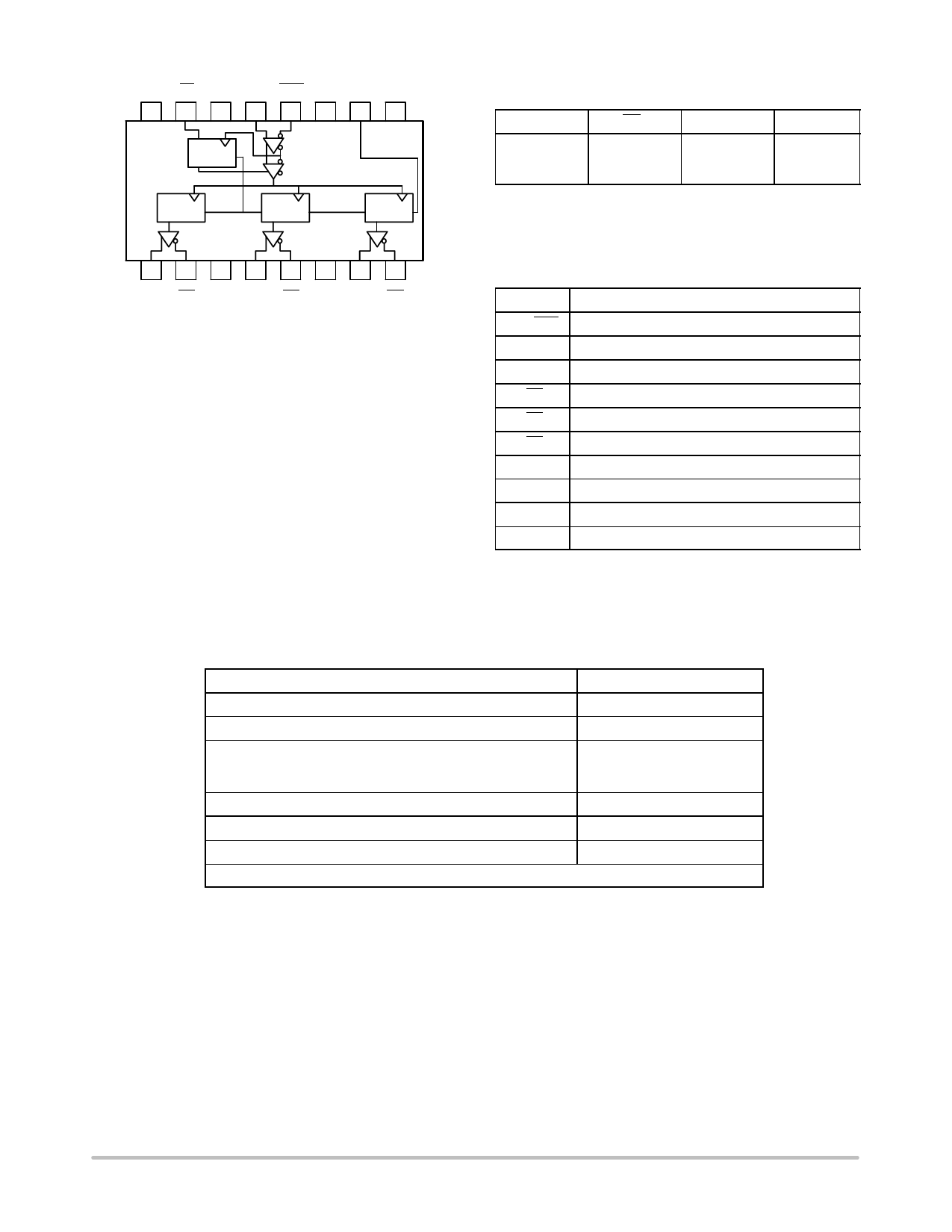
VCC EN NC CLK CLK VBB MR VEE
16 15 14 13 12 11 10 9
D
QR
÷2
QR
÷4
QR
÷8
QR
Table 1. FUNCTION TABLE
CLK*
EN*
MR*
Z
L
L
ZZ
H
L
X
X
H
*Pins will default low when left open.
Z = Low-to-High Transition
ZZ = High-to-Low Transition
12345678
Q0 Q0 VCC Q1 Q1 VCC Q2 Q2
*All VCC pins are tied together on the die.
Warning: All VCC and VEE pins must be externally connected
to Power Supply to guarantee proper operation.
Figure 1. Logic Diagram and Pinout Assignment
Table 2. PIN DESCRIPTION
Pin
Function
CLK, CLK ECL Diff Clock Inputs
EN
ECL Sync Enable
MR
ECL Master Reset
Q0, Q0
ECL Diff ÷2 Outputs
Q1, Q1
ECL Diff ÷4 Outputs
Q2, Q2
ECL Diff ÷8 Outputs
VBB
Reference Voltage Output
VCC
Positive Supply
VEE
Negative Supply
NC
No Connect
Function
Divide
Hold Q0−3
Reset Q0−3
Table 3. ATTRIBUTES
Characteristics
Value
Internal Input Pulldown Resistor
75 KW
Internal Input Pullup Resistor
N/A
ESD Protection
Human Body Model
Machine Model
Charge Device Model
> 1 KV
> 100 V
> 2 KV
Moisture Sensitivity (Note 1)
Level 1
Flammability Rating
Oxygen Index: 28 to 34
UL 94 V−0 @ 0.125 in
Transistor Count
191 Devices
Meets or Exceeds JEDEC Spec EIA/JESD78 IC Latchup Test
1. For additional Moisture Sensitivity information, refer to Application Note AND8003/D.
http://onsemi.com
2
Share Link: 