10WT10FNTRR データシートの表示(PDF) - Vishay Semiconductors
部品番号
コンポーネント説明
一致するリスト
10WT10FNTRR Datasheet PDF : 8 Pages
| |||
www.vishay.com
VS-10UT10, VS-10WT10FN
Vishay Semiconductors
ELECTRICAL SPECIFICATIONS
PARAMETER
SYMBOL
Forward voltage drop
VFM (1)(2)
Reverse leakage current
IRM (1)
Junction capacitance
Series inductance
Maximum voltage rate of change
CT
LS
dV/dt
Notes
(1) Pulse width < 300 μs, duty cycle < 2 %
(2) Only 1 anode pin connected
TEST CONDITIONS
5A
10 A
20 A
TJ = 25 °C
5A
10 A
20 A
TJ = 125 °C
TJ = 25 °C
TJ = 125 °C
VR = Rated VR
VR = 5 VDC (test signal range 100 kHz to 1 MHz), 25 °C
Measured lead to lead 5 mm from package body
Rated VR
THERMAL - MECHANICAL SPECIFICATIONS
PARAMETER
SYMBOL
Maximum junction and
storage temperature range
Maximum thermal resistance,
junction to case
TJ, TStg
RthJC DC operation
Typical thermal resistance,
case to heatsink
RthCS
TEST CONDITIONS
Approximate weight
Marking device
Case style I-PAK
Case style D-PAK
TYP.
0.630
0.735
0.840
0.530
0.615
0.730
-
-
400
8.0
-
MAX. UNITS
-
0.810
0.890
V
-
0.660
0.770
50
μA
4
mA
-
pF
-
nH
10 000 V/μs
VALUES
- 55 to 175
UNITS
°C
2
°C/W
0.3
0.3
g
0.01
oz.
10UT10
10WT10FN
100
TJ = 175 °C
10
TJ = 125 °C
TJ = 25 °C
1
0.2 0.4 0.6 0.8 1.0 1.2 1.4 1.6 1.8
VFM - Forward Voltage Drop (V)
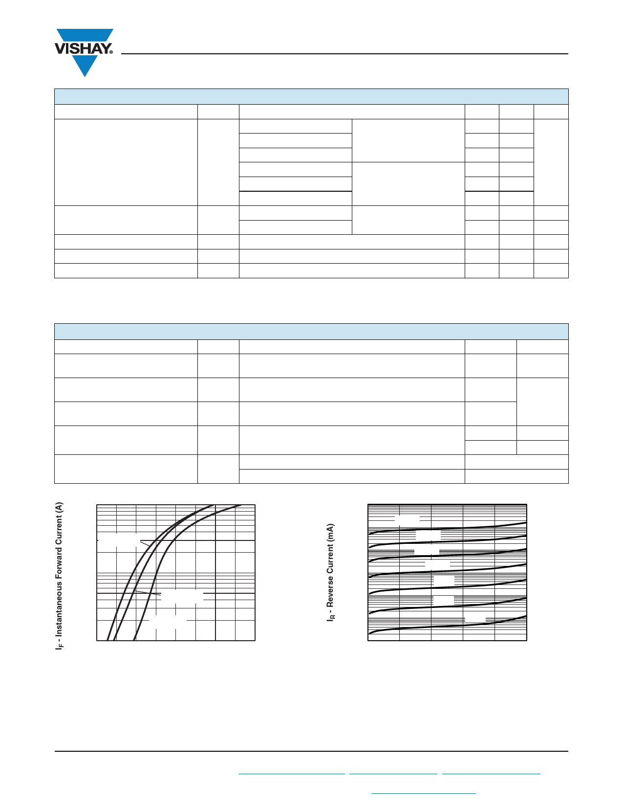
Fig. 1 - Maximum Forward Voltage Drop Characteristics
100
10
1
0.1
0.01
0.001
175 °C
150 °C
125 °C
100 °C
75 °C
50 °C
25 °C
0.0001
0
20
40
60
80
100
VR - Reverse Voltage (V)
Fig. 2 - Typical Values of Reverse Current vs.
Reverse Voltage
Revision: 10-Aug-11
2
Document Number: 94647
For technical questions within your region: DiodesAmericas@vishay.com, DiodesAsia@vishay.com, DiodesEurope@vishay.com
THIS DOCUMENT IS SUBJECT TO CHANGE WITHOUT NOTICE. THE PRODUCTS DESCRIBED HEREIN AND THIS DOCUMENT
ARE SUBJECT TO SPECIFIC DISCLAIMERS, SET FORTH AT www.vishay.com/doc?91000
Share Link: 