EM78P156EL データシートの表示(PDF) - Elan Microelectronics Corp
部品番号
コンポーネント説明
一致するリスト
EM78P156EL Datasheet PDF : 55 Pages
| |||
EM78P156EL
OTP ROM
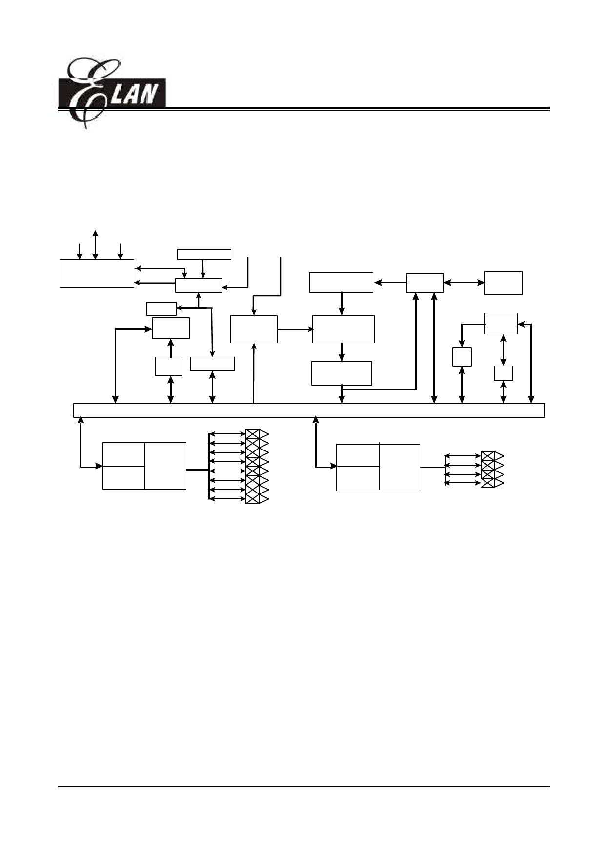
4. FUNCTION DESCRIPTION
OSCO
OSCI /RESET
Oscillator/Timing
Control
WDT timer TCC /INT
Prescaler
IOCA
RAM
Interrupt
Controller
R4
R1(TCC)
ROM
Instruction
Register
Instruction
Decoder
R2
Stack
ALU
R3
ACC
DATA & CONTROL BUS
P60//INT
P61
IOC6
R6
I/O
PORT 6
P62
P63
IOC5 I/O
P64
PORT 5
P65
R5
P50
P51
P52
P53
P66
P67
Fig. 2 Function Block Diagram
4.1 Operational Registers
1. R0 (Indirect Addressing Register)
R0 is not a physically implemented register. Its major function is to perform as an indirect addressing
pointer. Any instruction using R0 as a pointer actually accesses data pointed by the RAM Select
Register (R4).
2. R1 (Time Clock /Counter)
• Increased by an external signal edge, which is defined by TE bit (CONT-4) through the TCC pin, or
by the instruction cycle clock.
• Writable and readable as any other registers.
• Defined by resetting PAB(CONT-3).
• The prescaler is assigned to TCC, if the PAB bit (CONT-3) is reset.
• The contents of the prescaler counter will be cleared only when TCC register is written with a value.
This specification is subject to change without prior notice.
8
07.29.2004 (V1.3)
Share Link: 