8NB90FI データシートの表示(PDF) - STMicroelectronics
部品番号
コンポーネント説明
一致するリスト
8NB90FI Datasheet PDF : 9 Pages
| |||
ELECTRICAL CHARACTERISTICS (CONTINUED)
SWITCHING ON
Symbol
Parameter
td(on)
Turn-on Delay Time
tr
Rise Time
Qg
Total Gate Charge
Qgs
Gate-Source Charge
Qgd
Gate-Drain Charge
Test Conditions
VDD = 450 V, ID = 3.5 A
RG = 4.7Ω VGS = 10 V
(see test circuit, Figure 3)
VDD = 400V, ID = 9A,
VGS = 10V
SWITCHING OFF
Symbol
Parameter
tr(Voff)
Off-voltage Rise Time
tf
Fall Time
tc
Cross-over Time
Test Conditions
VDD = 720V, ID = 7.4 A,
RG = 4.7Ω, VGS = 10V
(see test circuit, Figure 5)
SOURCE DRAIN DIODE
Symbol
Parameter
Test Conditions
ISD
Source-drain Current
ISDM (2) Source-drain Current (pulsed)
VSD (1) Forward On Voltage
ISD = 8 A, VGS = 0
trr
Qrr
IRRM
Reverse Recovery Time
Reverse Recovery Charge
Reverse Recovery Current
ISD = 7.4 A, di/dt = 100A/µs,
VDD = 100V, Tj = 150°C
(see test circuit, Figure 5)
Note: 1. Pulsed: Pulse duration = 300 µs, duty cycle 1.5 %.
2. Pulse width limited by safe operating area.
STW8NB90 - STH8NB90FI
Min. Typ. Max. Unit
25
ns
12
ns
46
72
nC
12.5
nC
18
nC
Min.
Typ.
22
15
31
Max.
Unit
ns
ns
ns
Min. Typ. Max. Unit
8
A
32
A
1.6
V
700
ns
6.3
µC
18
A
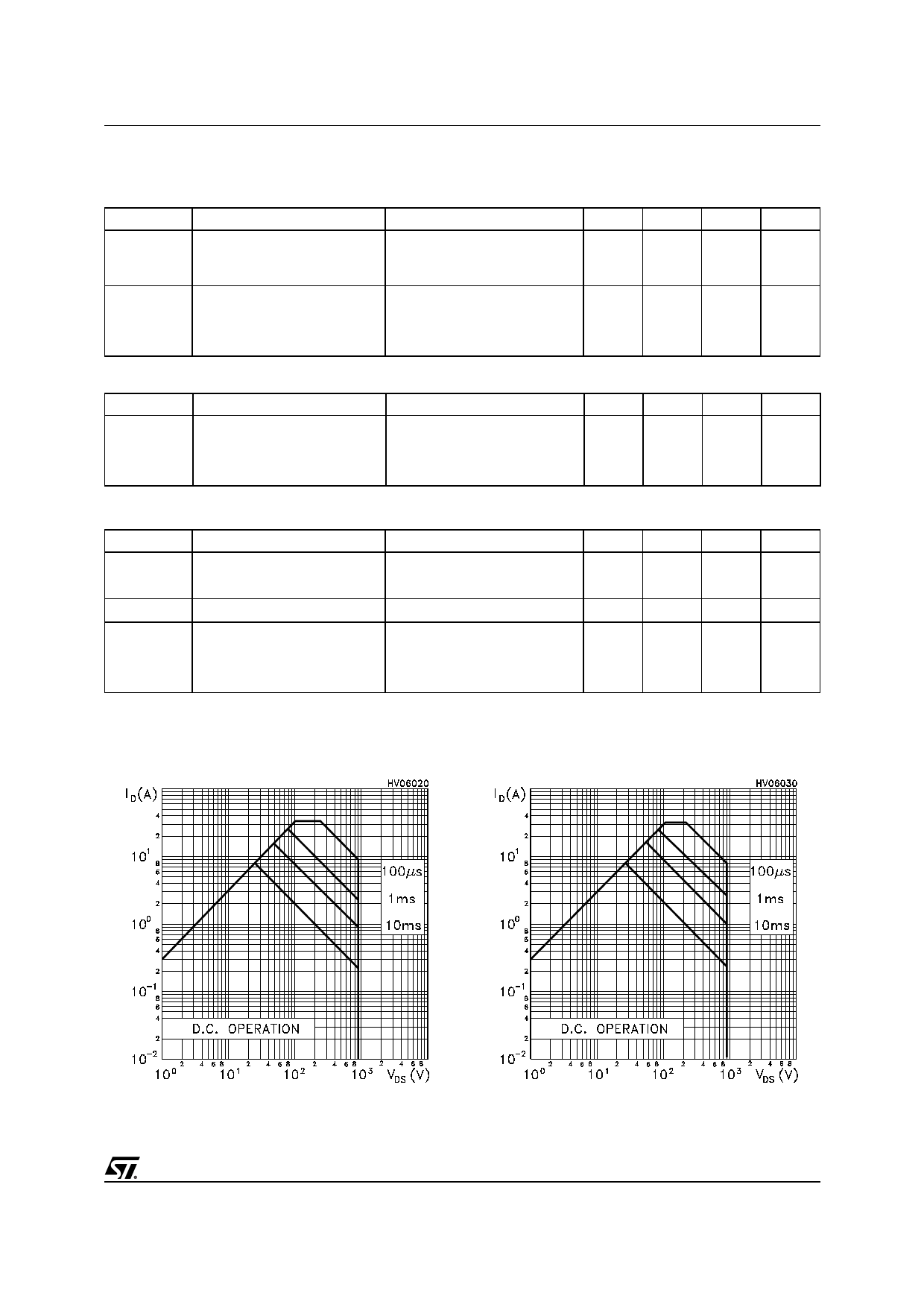
Safe Operating Area for TO-247
Safe Operating Area for ISOWATT218
3/9
Share Link: 