LIS244AL データシートの表示(PDF) - STMicroelectronics
部品番号
コンポーネント説明
一致するリスト
LIS244AL Datasheet PDF : 15 Pages
| |||
LIS244AL
Mechanical and electrical specifications
2.3
Absolute maximum ratings
Stresses above those listed as “absolute maximum ratings” may cause permanent damage
to the device. This is a stress rating only and functional operation of the device under these
conditions is not implied. Exposure to maximum rating conditions for extended periods may
affect device reliability.
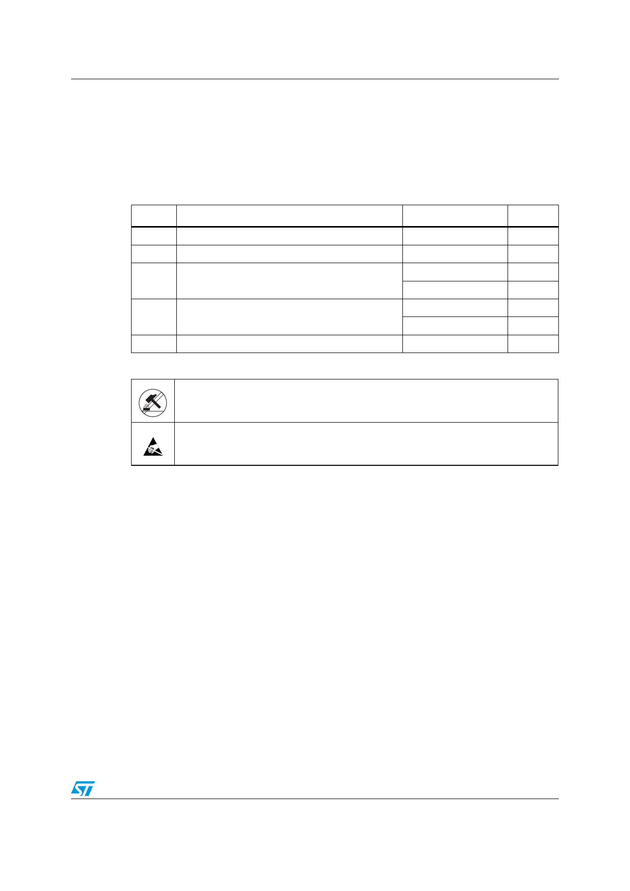
Table 5. Absolute maximum ratings
Symbol
Ratings
Vdd Supply voltage
Vin Input voltage on any control pin (ST)
APOW Acceleration (any axis, powered, Vdd=3.0V)
AUNP Acceleration (any axis, not powered)
TSTG Storage temperature range
Maximum value
Unit
-0.3 to 6
V
-0.3 to Vdd +0.3
V
3000g for 0.5 ms
10000g for 0.1 ms
3000g for 0.5 ms
10000g for 0.1 ms
-40 to +125
°C
This is a Mechanical Shock sensitive device, improper handling can cause permanent
damages to the part
This is an ESD sensitive device, improper handling can cause permanent damages to the
part
2.4
Terminology
Sensitivity describes the gain of the sensor and can be determined by applying 1g
acceleration to it. As the sensor can measure DC accelerations this can be done easily by
pointing the axis of interest towards the center of the earth, note the output value, rotate the
sensor by 180 degrees (point to the sky) and note the output value again thus applying ±1g
acceleration to the sensor. Subtracting the larger output value from the smaller one and
dividing the result by 2 will give the actual sensitivity of the sensor. This value changes very
little over temperature (see sensitivity change vs. temperature) and also very little over time.
The sensitivity tolerance describes the range of sensitivities of a large population of sensors.
Zero-g level describes the actual output signal if there is no acceleration present. A sensor
in a steady state on a horizontal surface will measure 0g in X axis and 0g in Y axis. The
output is ideally for a 3.0V powered sensor Vdd/2 = 1500mV. A deviation from ideal 0-g level
(1500mV in this case) is called Zero-g offset. Offset of precise MEMS sensors is to some
extend a result of stress to the sensor and therefore the offset can slightly change after
mounting the sensor onto a printed circuit board or exposing it to extensive mechanical
stress. Offset changes little over temperature - see “Zero-g level change vs. temperature” -
the Zero-g level of an individual sensor is very stable over lifetime. The Zero-g level
tolerance describes the range of Zero-g levels of a population of sensors.
7/15
Share Link: 