UPD4564323 データシートの表示(PDF) - NEC => Renesas Technology
部品番号
コンポーネント説明
一致するリスト
UPD4564323 Datasheet PDF : 84 Pages
| |||
µPD4564323 for Rev. E
2. Commands
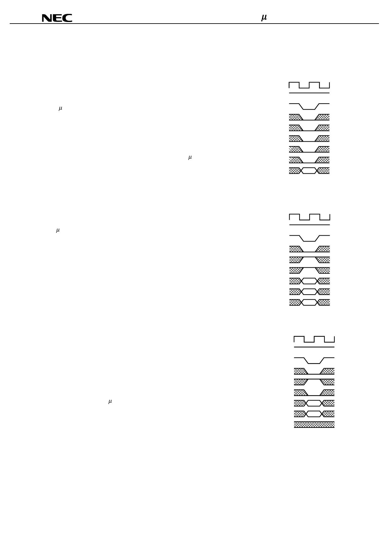
Mode register set command
Fig.1 Mode register set command
(/CS, /RAS, /CAS, /WE = Low)
The µPD4564323 has a mode register that defines how the device
operates. In this command, A0 through A10, BA0 and BA1 are the data input
pins. After power on, the mode register set command must be executed to
initialize the device.
The mode register can be set only when all banks are in idle state.
During 2 CLK (tRSC) following this command, the µPD4564323 cannot
accept any other commands.
CLK
CKE H
/CS
/RAS
/CAS
/WE
BA0, BA1
(Bank select)
A10
Add
Activate command
(/CS, /RAS = Low, /CAS, /WE = High)
The µPD4564323 has four banks, each with 4,096 rows.
This command activates the bank selected by BA0 and BA1 and a row
address selected by A0 through A10.
This command corresponds to a conventional DRAM’s /RAS falling.
Fig.2 Row address strobe and
bank activate command
CLK
CKE
/CS
/RAS
/CAS
/WE
BA0, BA1
(Bank select)
A10
Add
H
Row
Row
Precharge command
Fig.3 Precharge command
(/CS, /RAS, /WE = Low, /CAS = High)
This command begins precharge operation of the bank selected by BA0 and
BA1. When A10 is High, all banks are precharged, regardless of BA0 and
BA1. When A10 is Low, only the bank selected by BA0 and BA1 is
precharged.
After this command, the µPD4564323 can’t accept the activate command to
the precharging bank during tRP (precharge to activate command period).
This command corresponds to a conventional DRAM’s /RAS rising.
CLK
CKE H
/CS
/RAS
/CAS
/WE
BA0, BA1
(Bank select)
A10
(Precharge select)
Add
Data Sheet M14376EJ2V0DS00
9
Share Link: 