MC10H145FNR2 データシートの表示(PDF) - ON Semiconductor
部品番号
コンポーネント説明
一致するリスト
MC10H145FNR2 Datasheet PDF : 5 Pages
| |||
MC10H145
16 x 4 Bit Register File
(RAM)
The MC10H145 is a 16 x 4 bit register file. The active-low chip
select allows easy expansion.
The operating mode of the register file is controlled by the WE
input. When WE is “low” the device is in the write mode, the outputs
are “low” and the data present at Dn input is stored at the selected
address, when WE is “high,” the device is in the read mode − the data
state at the selected location is present at the Qn outputs.
• Address Access Time, 4.5 ns Typical
• Power Dissipation, 700 mW Typical
• Improved Noise Margin 150 mV (Over Operating Voltage and
Temperature Range)
• Voltage Compensated
• MECL 10K-Compatible
TRUTH TABLE
MODE
INPUT
OUTPUT
CS WE Dn
Qn
Write “0”
L
LL
L
Write “1”
L LH
L
Read
L HX
Q
Disabled
H XX
L
Q-State of Addressed Cell
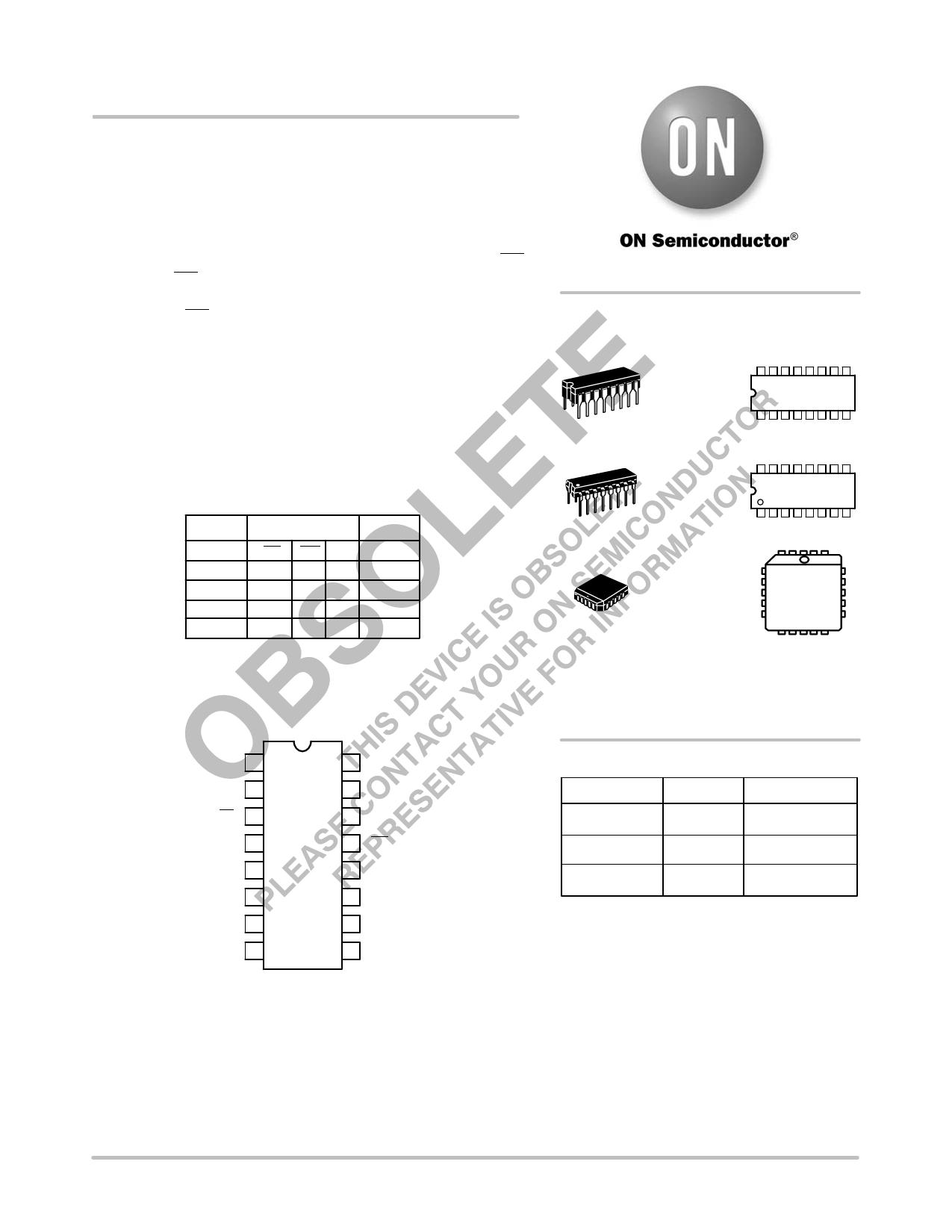
DIP
PIN ASSIGNMENT
Q1
1
Q0
2
CS
3
D1
4
D0
5
A3
6
A2
7
VEE
8
16
VCC
15
Q2
14
Q3
13
WE
12
D3
11
D2
10
A0
9
A1
Pin assignment is for Dual−in−Line Package.
For PLCC pin assignment, see the Pin Conversion Tables
on page 6−11 of the Motorola MECL Data Book (DL122/D).
http://onsemi.com
CDIP−16
L SUFFIX
CASE 620
PDIP−16
P SUFFIX
CASE 648
PLCC−20
FN SUFFIX
CASE 775
MARKING
DIAGRAMS
16
MC10H145L
AWLYYWW
1
16
MC10H145P
AWLYYWW
1
1
10H145
AWLYYWW
A = Assembly Location
WL = Wafer Lot
YY = Year
WW = Work Week
ORDERING INFORMATION
Device
Package
Shipping
MC10H145L
CDIP−16
25 Units/Rail
MC10H145P
PDIP−16
25 Units/Rail
MC10H145FN PLCC−20
xx Units/Rail
© Semiconductor Components Industries, LLC, 2006
1
June, 2006 − Rev. 7
Publication Order Number:
MC10H145/D
Share Link: 