MAX6520 データシートの表示(PDF) - Maxim Integrated
部品番号
コンポーネント説明
一致するリスト
MAX6520 Datasheet PDF : 6 Pages
| |||
50ppm/°C, SOT23, 3-Terminal,
1.2V Voltage Reference
_____________________Pin Description
PIN
NAME
FUNCTION
1
VIN
Input Voltage
2
VOUT Reference Output
3
GND Ground
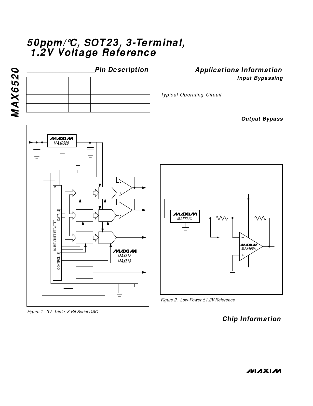
+3V VIN
1
0.1µF
MAX6520
3
VOUT
2
0.01µF
__________Applications Information
Input Bypassing
For the best line-transient performance, decouple the
input with a 0.1µF ceramic capacitor as shown in the
Typical Operating Circuit. Locate the capacitor as
close to the device pin as possible. Where transient
performance is less important, no capacitor is neces-
sary.
Output Bypass
The MAX6520 performs well without an output decou-
pling capacitor. If your application requires an output
charge reservoir (e.g., to decouple the reference from
the input of a DAC), then make sure that the total output
capacitive load does not exceed 10nF.
DIN
1
SCLK
3
CS REFAB
REFC
2
12 11
DAC
LATCH A
DAC A
DAC
LATCH B
DAC B
OUTA
8
OUTB
9
DAC
LATCH C
DAC C
OUTC
10
LATCH
4
RESET
MAX512
MAX513
LOUT
14
5
7
6
VDD VSS
GND
Figure 1. 3V, Triple, 8-Bit Serial DAC
+3V
VIN
VOUT
1 MAX6520 2
3
R
R
+1.2V
27
MAX406A
3
4
-3V
6 -1.2V
Figure 2. Low-Power ±1.2V Reference
___________________Chip Information
TRANSISTOR COUNT: 39
4 _______________________________________________________________________________________
Share Link: 