CY2305(2002) データシートの表示(PDF) - Cypress Semiconductor
部品番号
コンポーネント説明
一致するリスト
CY2305 Datasheet PDF : 13 Pages
| |||
CY2305
CY2309
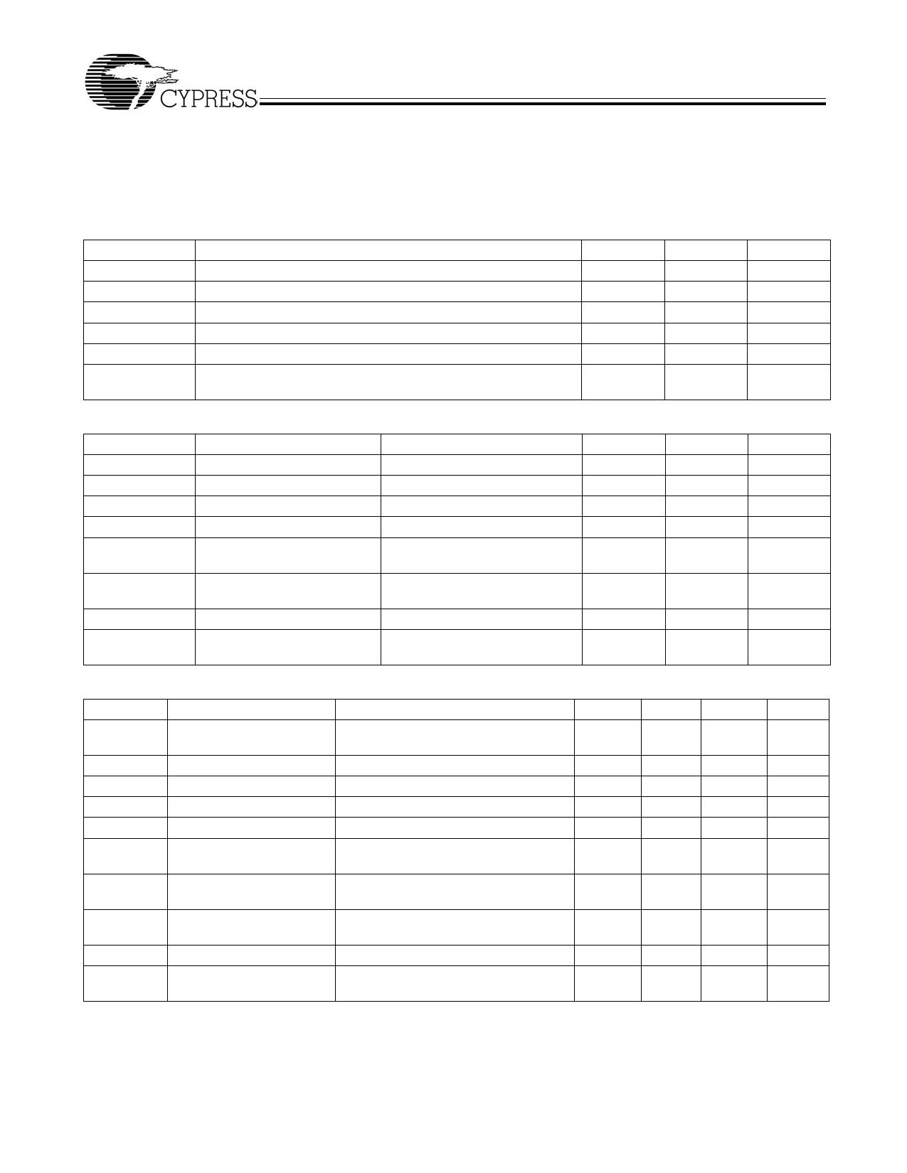
Maximum Ratings
Supply Voltage to Ground Potential ............... –0.5V to +7.0V Storage Temperature ................................. –65°C to +150°C
DC Input Voltage (Except REF) ............–0.5V to VDD + 0.5V Junction Temperature ................................................. 150°C
DC Input Voltage REF......................................... –0.5V to 7V Static Discharge Voltage
(per MIL-STD-883, Method 3015) ........................... > 2,000V
Operating Conditions for CY2305SC-XX and CY2309SC-XX Commercial Temperature Devices
Parameter
Description
Min.
Max.
Unit
VDD
Supply Voltage
3.0
3.6
V
TA
Operating Temperature (Ambient Temperature)
0
70
°C
CL
Load Capacitance, below 100 MHz
30
pF
CL
Load Capacitance, from 100 MHz to 133 MHz
10
pF
CIN
Input Capacitance
7
pF
Power-up time for all VDD's to reach minimum specified voltage
tPU
(power ramps must be monotonic)
0.05
50
ms
Electrical Characteristics for CY2305SC-XX and CY2309SC-XX Commercial Temperature Devices
Parameter
VIL
VIH
IIL
IIH
VOL
VOH
IDD (PD mode)
IDD
Description
Input LOW Voltage[5]
Input HIGH Voltage[5]
Input LOW Current
Input HIGH Current
Output LOW Voltage[6]
Output HIGH Voltage[6]
Power Down Supply Current
Supply Current
Test Conditions
VIN = 0V
VIN = VDD
IOL = 8 mA (–1)
IOH = 12 mA (–1H)
IOH = –8 mA (–1)
IOL = –12 mA (–1H)
REF = 0 MHz
Unloaded outputs at 66.67 MHz,
SEL inputs at VDD
Min.
2.0
2.4
Max.
0.8
50.0
100.0
0.4
12.0
32.0
Unit
V
V
µA
µA
V
V
µA
mA
Switching Characteristics for CY2305SC-1and CY2309SC-1 Commercial Temperature Devices[7]
Parameter
Name
Test Conditions
Min.
Typ.
Max.
Unit
t1
Output Frequency
30-pF load
10-pF load
10
100
MHz
10
133.33 MHz
Duty Cycle[6] = t2 ÷ t1
Measured at 1.4V, Fout = 66.67 MHz
40.0
50.0
60.0
%
t3
Rise Time[6]
Measured between 0.8V and 2.0V
2.50
ns
t4
Fall Time[6]
Measured between 0.8V and 2.0V
t5
Output to Output Skew[6] All outputs equally loaded
2.50
ns
250
ps
t6A
Delay, REF Rising Edge to
CLKOUT Rising Edge[6]
Measured at VDD/2
0
±350
ps
t6B
t7
tJ
tLOCK
Delay, REF Rising Edge to
CLKOUT Rising Edge[6]
Measured at VDD/2. Measured in PLL
Bypass Mode, CY2309 device only.
1
Device to Device Skew[6] Measured at VDD/2 on the CLKOUT pins
of devices
Cycle to Cycle Jitter[6]
Measured at 66.67 MHz, loaded outputs
PLL Lock Time[6]
Stable power supply, valid clock
presented on REF pin
5
8.7
ns
0
700
ps
200
ps
1.0
ms
Notes:
5. REF input has a threshold voltage of VDD/2.
6. Parameter is guaranteed by design and characterization. Not 100% tested in production.
7. All parameters specified with loaded outputs.
Document #: 38-07140 Rev. *C
Page 4 of 13
Share Link: 