CY2309(2002) データシートの表示(PDF) - Cypress Semiconductor
部品番号
コンポーネント説明
一致するリスト
CY2309 Datasheet PDF : 13 Pages
| |||
CY2305
CY2309
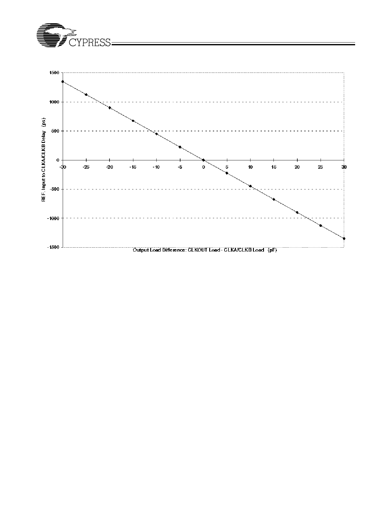
REF. Input to CLKA/CLKB Delay vs. Loading Difference between CLKOUT and CLKA/CLKB Pins
Zero Delay and Skew Control
All outputs should be uniformly loaded to achieve Zero Delay
between the input and output. Since the CLKOUT pin is the
internal feedback to the PLL, its relative loading can adjust the
input-output delay. This is shown in the above graph.
For applications requiring zero input-output delay, all outputs,
including CLKOUT, must be equally loaded. Even if CLKOUT
is not used, it must have a capacitive load, equal to that on
other outputs, for obtaining zero input-output delay. If input to
output delay adjustments are required, use the above graph to
calculate loading differences between the CLKOUT pin and
other outputs.
For zero output-output skew, be sure to load all outputs
equally. For further information refer to the application note
entitled “CY2305 and CY2309 as PCI and SDRAM Buffers.”
Document #: 38-07140 Rev. *C
Page 3 of 13
Share Link: 