CS5460A-BSZ データシートの表示(PDF) - Cirrus Logic
部品番号
コンポーネント説明
一致するリスト
CS5460A-BSZ Datasheet PDF : 54 Pages
| |||
CS5460A
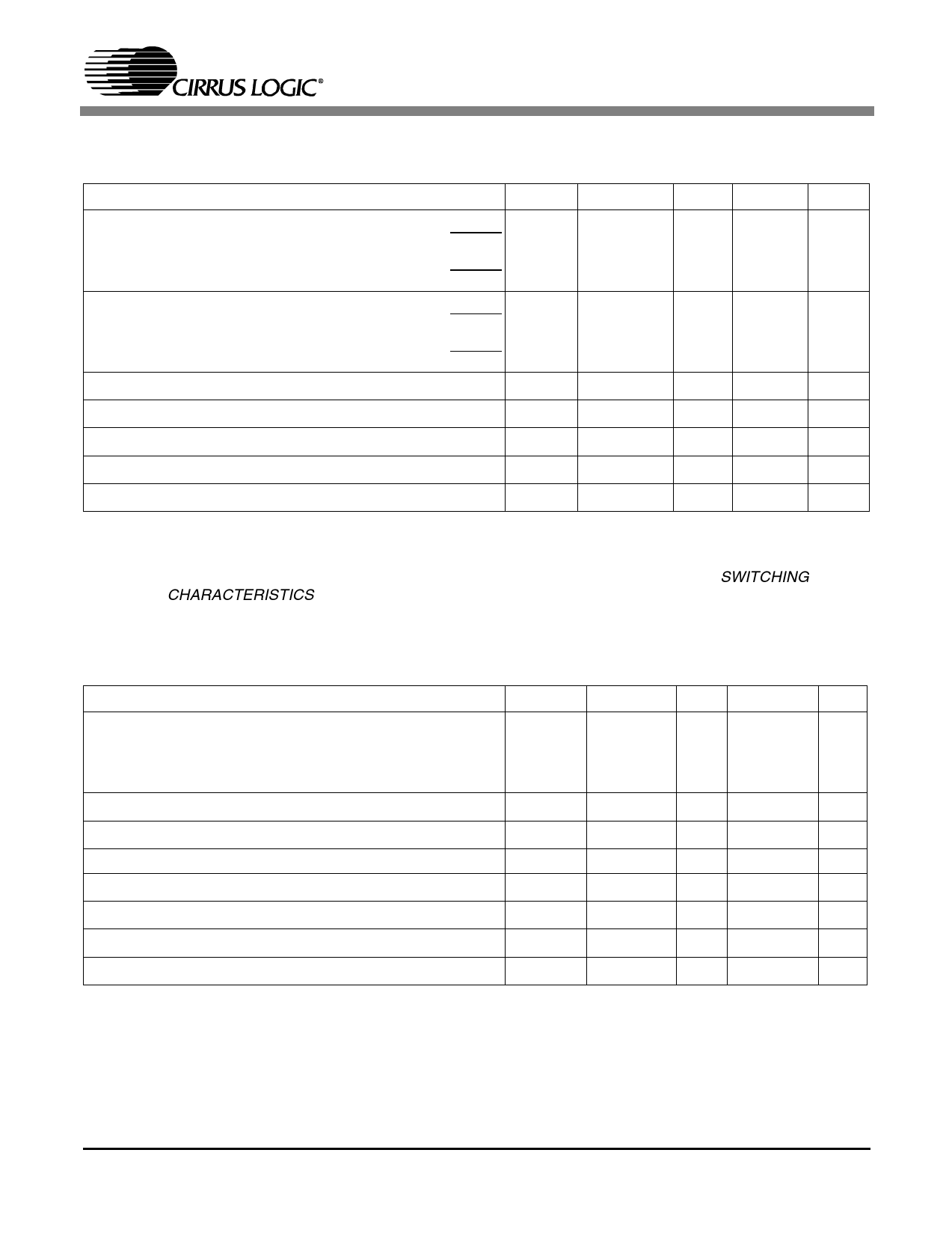
3.3 V DIGITAL CHARACTERISTICS
(TA = -40 °C to +85 °C; VA+ = 5 V ±10%, VD+ = 3.3 V ±10%; VA-, DGND = 0 V) (See Notes 3, 4, and 13)
Parameter
Symbol
Min
Typ Max Unit
High-Level Input Voltage
VIH
All Pins Except XIN, XOUT, SCLK, and RESET
0.6 VD+
-
-
V
XIN
(VD+) - 0.5 -
-
V
SCLK and RESET
0.8 VD+
-
-
V
Low-Level Input Voltage
VIL
All Pins Except XIN, XOUT, SCLK, and RESET
-
-
0.48
V
XIN
-
-
0.3
V
SCLK and RESET
-
- 0.2 VD+ V
High-Level Output Voltage (except XIN, XOUT) Iout = +5 mA VOH (VD+) - 1.0 -
-
V
Low-Level Output Voltage (except XIN, XOUT) Iout = -5 mA VOL
-
-
0.4
V
Input Leakage Current
(Note 14) Iin
-
±1
±10
µA
3-State Leakage Current
IOZ
-
-
±10
µA
Digital Output Pin Capacitance
Cout
-
5
-
pF
Notes: 15. All measurements performed under static conditions.
16. If VD+ = 3 V and if XIN input is generated using crystal, then XIN frequency must remain between
2.5 MHz - 5.0 MHz. If using oscillator, full XIN frequency range is available, see SWITCHING
CHARACTERISTICS.
ABSOLUTE MAXIMUM RATINGS
(DGND = 0 V; See Note 17) WARNING: Operation at or beyond these limits may result in permanent damage to
the device. Normal operation is not guaranteed at these extremes.
Parameter
Symbol
Min
Typ
Max
Unit
DC Power Supplies
(Notes 18 and 19)
Positive Digital
Positive Analog
Negative Analog
VD+
VA+
VA-
-0.3
-
-0.3
-
+0.3
-
+6.0
V
+6.0
V
-6.0
V
Input Current, Any Pin Except Supplies(Note 20, 21, and 22) IIN
-
-
±10
mA
Output Current
IOUT
-
-
±25
mA
Power Dissipation
(Note 23) PD
-
-
500
mW
Analog Input Voltage
All Analog Pins VINA (VA-) - 0.3 - (VA+) + 0.3 V
Digital Input Voltage
All Digital Pins VIND DGND - 0.3 - (VD+) + 0.3 V
Ambient Operating Temperature
TA
-40
-
85
°C
Storage Temperature
Tstg
-65
-
150
°C
Notes: 17.
18.
19.
20.
21.
22.
23.
All voltages with respect to ground.
VA+ and VA- must satisfy {(VA+) - (VA-)} ≤ +6.0 V.
VD+ and VA- must satisfy {(VD+) - (VA-)} ≤ +6.0 V.
Applies to all pins including continuous over-voltage conditions at the analog input (AIN) pins.
Transient current of up to 100 mA will not cause SCR latch-up.
Maximum DC input current for a power supply pin is ±50 mA.
Total power dissipation, including all input currents and output currents.
8
Share Link: 