54HC244 データシートの表示(PDF) - Motorola => Freescale
部品番号
コンポーネント説明
一致するリスト
54HC244 Datasheet PDF : 8 Pages
| |||
MC54/74HC244A
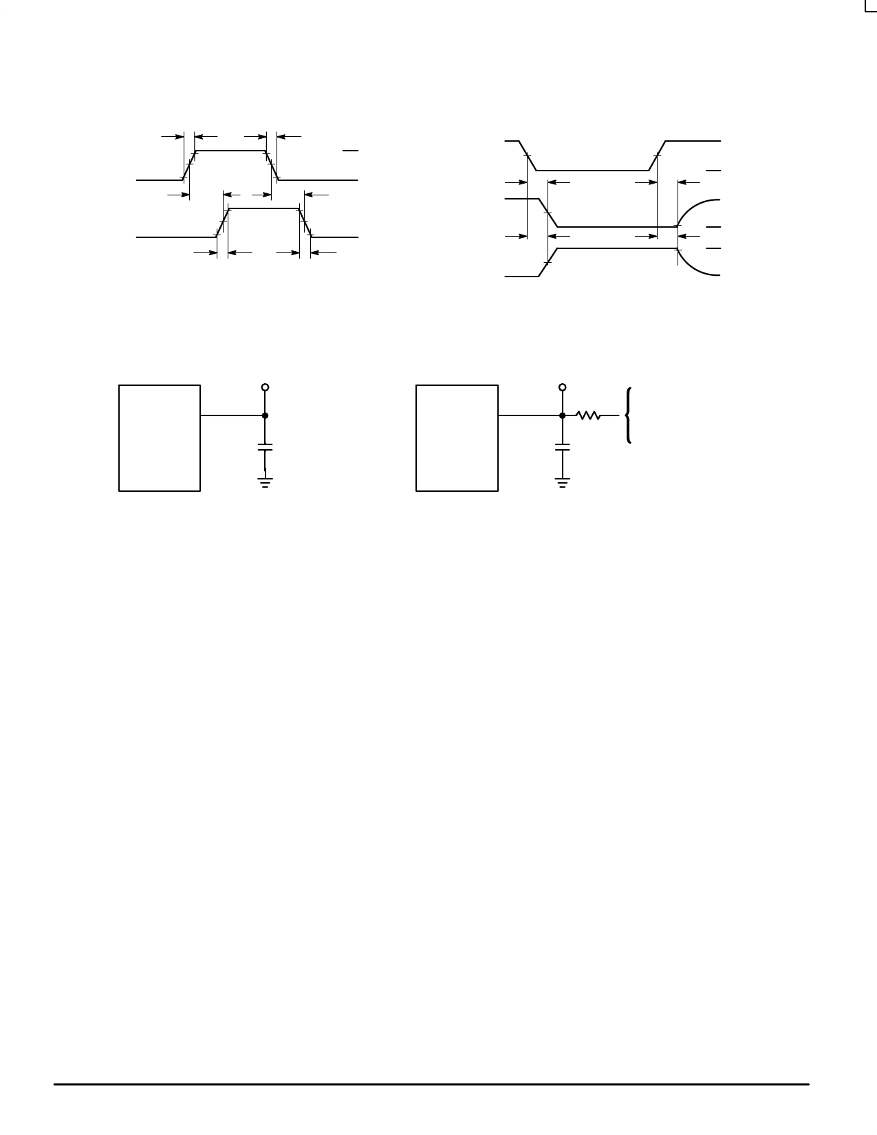
SWITCHING WAVEFORMS
tr
DATA INPUT
A OR B
tPLH
OUTPUT
YA OR YB
90%
50%
10%
90%
50%
10%
tTLH
tf
VCC
GND
tPHL
tTHL
Figure 1.
ENABLE
A OR B
OUTPUT Y
OUTPUT Y
50%
tPZL tPLZ
50%
tPZH tPHZ
50%
Figure 2.
VCC
GND
HIGH
IMPEDANCE
10% VOL
90% VOH
HIGH
IMPEDANCE
TEST CIRCUITS
DEVICE
UNDER
TEST
TEST POINT
OUTPUT
CL*
DEVICE
UNDER
TEST
TEST POINT
OUTPUT
1 kΩ
CL*
CONNECT TO VCC WHEN
TESTING tPLZ AND tPZL.
CONNECT TO GND WHEN
TESTING tPHZ AND tPZH.
* Includes all probe and jig capacitance
Figure 3. Test Circuit
* Includes all probe and jig capacitance
Figure 4. Test Circuit
PIN DESCRIPTIONS
INPUTS
A1, A2, A3, A4, B1, B2, B3, B4
(Pins 2, 4, 6, 8, 11, 13, 15, 17)
Data input pins. Data on these pins appear in noninverted
form on the corresponding Y outputs, when the outputs are
enabled.
CONTROLS
Enable A, Enable B (Pins 1, 19)
Output enables (active–low). When a low level is applied
to these pins, the outputs are enabled and the devices func-
tion as noninverting buffers. When a high level is applied, the
outputs assume the high impedance state.
OUTPUTS
YA1, YA2, YA3, YA4, YB1, YB2, YB3, YB4
(Pins 18, 16, 14, 12, 9, 7, 5, 3)
Device outputs. Depending upon the state of the output–
enable pins, these outputs are either noninverting outputs or
high–impedance outputs.
MOTOROLA
4
High–Speed CMOS Logic Data
DL129 — Rev 6
Share Link: 