GL901RX データシートの表示(PDF) - Genesys Logic
部品番号
コンポーネント説明
一致するリスト
GL901RX Datasheet PDF : 15 Pages
| |||
GL901Rx 1.1
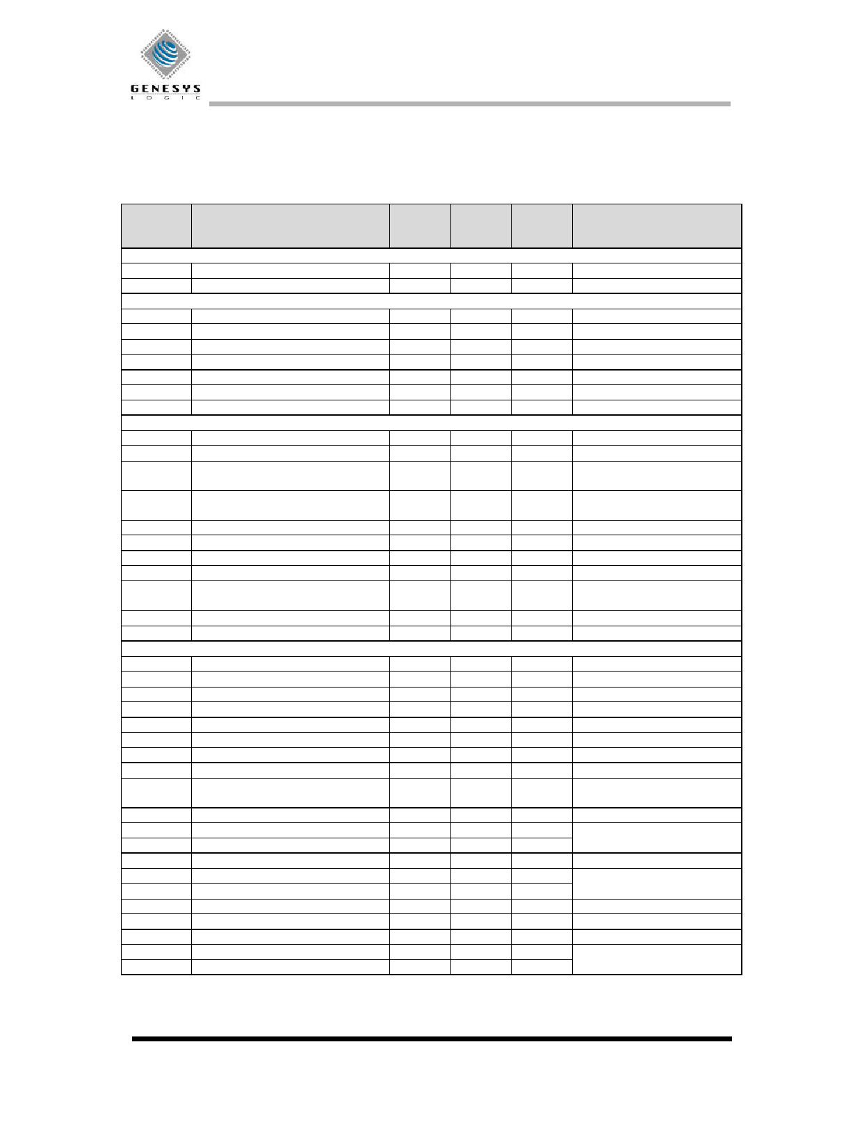
5. Electrical Characteristics
Table 5-1: Electrical Characteristics
Symbol Operating Temperature = 0 to 85°C;
FOSC = 6MHz, VCC = 4.4 to 5.5V
Min
Characteristic
Max
Units
Conditions
General
ICC
Operating supply current
ISB
Supply current – suspend mode
USB Interface
20
mA
360
µA
See note 1
VOH
VOL
VDI
VCM
VSE
ILO
V3.3
Static output high
Static output low
Differential input sensitivity
Differential common mode range
Single ended receiver threshold
Hi-Z state data line leakage
Regulator supply voltage
GPIO Interface
2.8
3.6
0.3
0.2
0.8
2.5
0.8
2.0
-10
+10
3.0
3.6
V
RL of 15KΩ to GND
V
RL of 15KΩ to V3.3
V
|(D+) – (D-)|
V
Include VDI range
V
V
0V < VIN < 3.3V
V
IL = 4mA
RUP
RDOWN
VOH1
PORT2.2-4 pull-up resistance
PORT1.0-7 pull-down resistance
Static output high for PORT1.2-4,
PORT2.0-7
68
120
KΩ
4
32
KΩ
Code option
2.4
V
VCC = 5V; IOH = 4mA
VOL1
Static output low for PORT1.2-4,
PORT2.0-7
0.4
V
VCC = 5V; IOL = 4mA
VOH2
VOL2
VIH
VIL
ISINK1
Static output high for PORT1.0-1
Static output low for PORT1.0-1
Static input high
Static input low
Sink current for PORT1.2-4,
PORT2.0-7
2.4
V
VCC = 5V; IOH = 20mA
0.4
V
VCC = 5V; IOL = 20mA
2.0
V
VCC = 5V
0.9
V
VCC = 5V
4
mA
VOUT = 0.4V;
ISINK2
IIN
Sink current for PORT1.0-1
Input leakage current
USB Low-speed Source
20
mA
VOUT = 0.4V;
-1
+1
µA
VOUT = 0V or VCC
fOP
Internal operating frequency
Transition time
1.5
1.5
MHz
tR
tF
tRFM
VCRS
tDRATE
Rise time
Fall time
Rise/Fall time matching
Output signal crossover voltage
Low speed data rate
75
75
80
1.3
1.4775
676.8
300
300
120
2.0
1.5225
666.0
ns
CL = 50pF
ns
CL = 350pF
ns
CL = 50pF
ns
CL = 350pF
%
tR / tF
V
Mbs 1.5Mbs ± 1.5%
ns
Source differential driver jitter
tUDJ1
To next transition
tUDJ2
For paired transition
Receiver data jitter tolerance
-25
25
ns
CL = 350pF measured at
-10
10
ns
crossover point
tDJR1
tDJR2
tEOPT
tDEOP
To next transition
-75
75
For paired transition
-45
45
Source EOP width
1.25
1.50
Differential to EOP transition skew
-40
100
Receiver EOP width
ns
CL = 350pF measured at
ns
crossover point
µs
Measured at crossover point
ns
Measured at crossover point
tEOPR1
Must reject as EOP
330
ns
Measured at crossover point
tEOPR2
Must accept
675
ns
Notes: ISB measured with USB in suspend mode; using external square wave clock source (FOSC = 6MHz); transceiver pull-up
resistor of 1.5KΩ between V3.3 and D- and 15KΩ termination resistors on D+ and D- pins; no port pins sourcing current. The ISB
value is including power consumed by external resistors.
©2000-2001 Genesys Logic Inc.—All rights reserved
-13
Share Link: 