FS6158-01 データシートの表示(PDF) - AMI Semiconductor
部品番号
コンポーネント説明
一致するリスト
FS6158-01 Datasheet PDF : 14 Pages
| |||
FS6158-01
Two-Way/Four Way Motherboard Clock Generator/Buffer IC
2.0 Programming Information
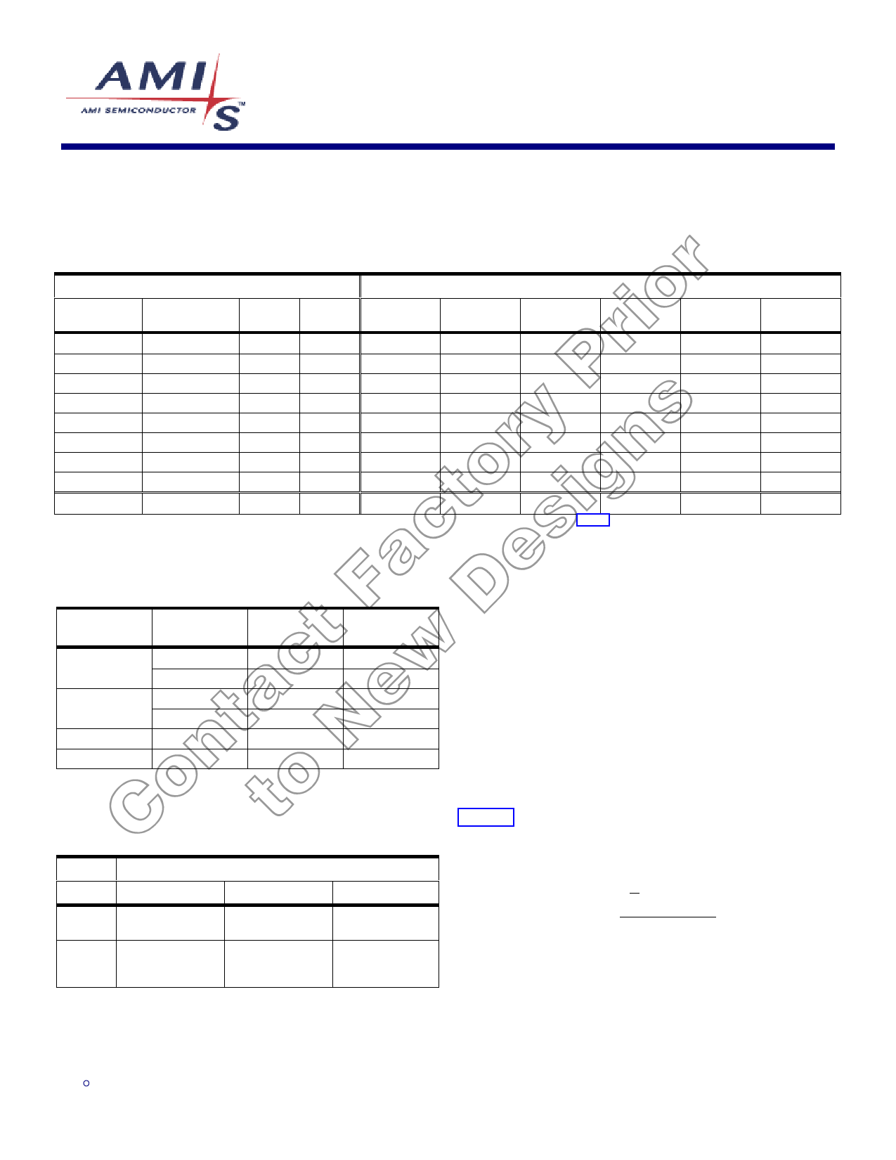
Table 3: Function/Clock Enable Configuration
CONTROL INPUTS (2)
CLOCK OUTPUTS (MHz)
PWR_DWN# SEL133/100#
SEL_A
SEL_B HOST_P1:6 HOST_N1:6
MREF_P,
MREF_N
66REF
APIC_0:2
(optional)
14REF
1
0
0
0
100.00
100.00
50.00
66.67
33.33
14.318
1
0
0
1
100.00
100.00
low (1)
low (1)
low (1)
low (1)
1
0
1
0
reserved
reserved
reserved
reserved
reserved
reserved
1
0
1
1
tristate
tristate
tristate
tristate
tristate
tristate
1
1
0
0
133.33
133.33
66.67
66.67
33.33
14.318
1
1
0
1
reserved
reserved
reserved
reserved
reserved
reserved
1
1
1
0
reserved
reserved
reserved
reserved
reserved
reserved
1
1
1
1
XIN÷2
XIN÷2
XIN÷4
XIN÷4
XIN÷8
XIN
0
X
X
X
2× IREF
tristate
low
low
low
low
1. Certain clock outputs may be disabled through a combination of SEL_A, SEL_B, and SEL133/100# logic states as defined in Table 3. Enabled clocks will continue to run while disabled clocks
are stopped low. Note that if clocks are disabled while active, glitches may occur.
Table 4: Synthesis Error
CLOCK
TARGET
(MHz)
ACTUAL
(MHz)
DEVIATION
(ppm)
HOST_P1:6,
HOST_N1:6
100.0000
133.3333
99.9963
133.3072
-36.657
-195.924
MREF_P,
MREF_N
50.0000
66.6667
49.9982
66.6536
-36.657
-195.924
66REF
66.6667
66.6642
-36.657
APIC_0:2
33.3333
33.3321
-36.657
1. 48MHz USB clock is required to be +167ppm off from 48.000MHz to conform to USB
standards.
2. Spread spectrum is disabled
Table 5: APICON Control
APICON
PIN 47
0
1
FREQUENCY SELECT CONTROL / APIC CLOCKS
PIN 21
PIN 22
PIN 23
SEL_A Input
(LVTTL)
APIC_0 Output /
SEL_A Latched
Input
SEL_B Input
(LVTTL)
APIC_1 Output /
SEL_B Latched
Input
SS_EN# Input
(LVTTL)
APIC_2 Output /
SS_EN# Latched
Input
3.0 HOST Buffer Current Control
The current supplied at the HOST outputs is controlled by
two parameters:
1) the value of the programming resistor from the IREF
pin to ground (VSS), and
2) the multiplier factor determined by the logic setting of
the ISEL_0 and ISEL_1 pins.
3.1 Current Reference
The HOST output current is a mirrored and scaled copy
of the reference current flowing through the programming
resistor on the IREF pin. Conceptually, the circuit given in
Figure 2 shows how the mirror current is generated.
The voltage that appears at the IREF pin is one-third of
the voltage at the VDD_I pin. The reference current is
çæ 1 × VDD_I÷ö
I REF = è 3 RIREF
ø.
3.2 Current Scaling
The mirrored reference current can be increased by
adding one or more copies of the mirror current together.
The additional current is controlled by the logic settings
on the ISEL_0 and ISEL_1 pins.
ISO9001
3
2.26.02
Share Link: 