MP9141 データシートの表示(PDF) - Monolithic Power Systems
部品番号
コンポーネント説明
一致するリスト
MP9141 Datasheet PDF : 10 Pages
| |||
MP9141 – 1.8A STEP-DOWN DC TO DC CONVERTER
MPS CONFIDENTIAL AND PROPRIETARY INFORMATION– INTERNAL USE ONLY
Output Capacitor
The output capacitor is required to maintain the
DC output voltage. Low ESR capacitors are
preferred to keep the output voltage ripple low.
The characteristics of the output capacitor also
affect the stability of the regulation control
system. Ceramic, tantalum or low ESR
electrolytic capacitors are recommended. In the
case of ceramic capacitors, the impedance at
the switching frequency is dominated by the
capacitance and so the output voltage ripple is
mostly independent of the ESR. The output
voltage ripple is estimated to be:
VRIPPLE
≅ 1.4 × VIN
×
⎜⎜⎝⎛
fLC
f
⎟⎟⎠⎞ 2
Where VRIPPLE is the output ripple voltage, VIN is
the input voltage, fLC is the resonant frequency
of the LC filter and f is the switching frequency.
In the case of tantalum or low-ESR electrolytic
capacitors, the ESR dominates the impedance
at the switching frequency, and so the output
ripple is calculated as:
VRIPPLE ≅ ∆I × RESR
Where VRIPPLE is the output voltage ripple, ∆I is
the inductor ripple current and RESR is the
equivalent series resistance of the output
capacitors.
Output Rectifier Diode
The output rectifier diode supplies the current to
the inductor when the high-side switch is off. To
reduce losses due to the diode forward voltage
and recovery times, use a Schottky rectifier.
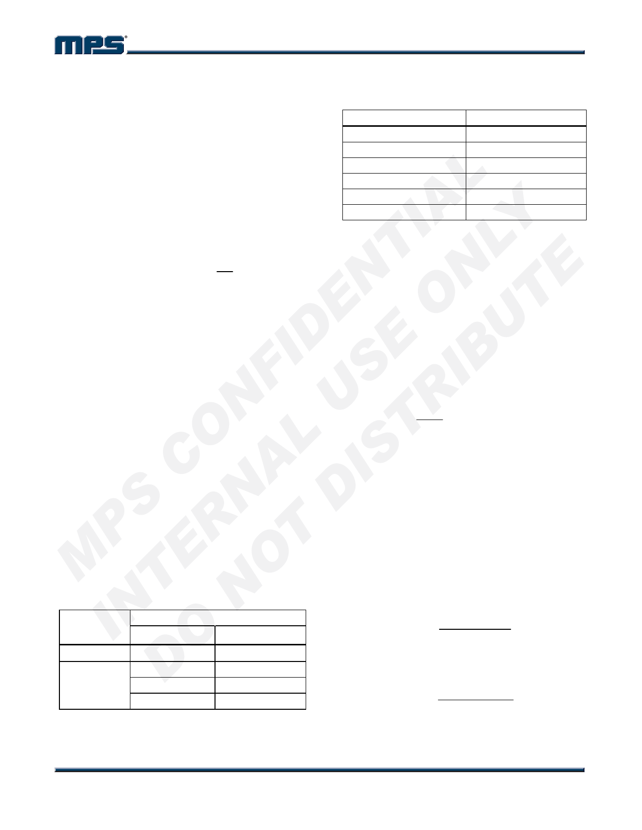
Table 2 provides the Schottky rectifier part
numbers based on the maximum input voltage
and current rating.
Table 2—Schottky Rectifier Selection Guide
Table 3 lists some rectifier manufacturers.
Table 3—Schottky Diode Manufacturers
Vendor
Web Site
Diodes, Inc.
www.diodes.com
Fairchild Semiconductor www.fairchildsemi.com
General Semiconductor www.gensemi.com
International Rectifier www.irf.com
On Semiconductor
www.onsemi.com
Pan Jit International
www.panjit.com.tw
Choose a rectifier whose maximum reverse
voltage rating is greater than the maximum
input voltage, and has a current rating greater
than the maximum load current.
Compensation
The system stability is controlled through the
COMP pin. COMP is the output of the internal
transconductance error amplifier. A series
capacitor-resistor combination sets a pole-zero
combination to control the characteristics of the
control system.
The DC loop gain is:
A VDC
=
VFB
VOUT
× A VEA
× GCS × RLOAD
Where VFB is the feedback threshold voltage,
VOUT is the desired output regulation voltage,
AVEA is the transconductance error amplifier
voltage gain, GCS is the current sense gain
(roughly the output current divided by the
voltage at COMP) equal to 1.95 A/V and RLOAD
is the load resistance (VOUT / IOUT where IOUT is
the output load current)
The system has two poles of importance, one is
due to the compensation capacitor (C5), and
the other is due to the output capacitor (C7).
These are:
VIN (Max)
15V
20V
1.8A Load Current
Part Number
Vendor
30BQ015
4
B220
1
SK23
6
SR32
6
fP1
=
2π ×
GEA
A VEA
× C5
Where P1 is the first pole, and GEA is the error
amplifier transconductance (770µA/V), and:
fP2
=
1
2π × RLOAD
× C7
MP9141 Rev. 1.11
www.MonolithicPower.com
7
4/18/2011
MPS Proprietary Information. Patent Protected. Unauthorized Photocopy and Duplication Prohibited.
© 2011 MPS. All Rights Reserved.
Share Link: 