MP3213DH-LF-Z データシートの表示(PDF) - Monolithic Power Systems
部品番号
コンポーネント説明
一致するリスト
MP3213DH-LF-Z Datasheet PDF : 10 Pages
| |||
MP3213 – 700KHZ/1.3MHZ BOOST CONVERTER WITH A 3.5A SWITCH
Layout Consideration
High frequency switching regulators require very
careful layout for stable operation and low noise.
All components must be placed as close to the IC
as possible. Keep the path between the SW pin,
output diode, output capacitor and GND pin
extremely short for minimal noise and ringing. The
input capacitor must be placed close to the IN pin
for best decoupling. All feedback components
must be kept close to the FB pin to prevent noise
injection on the FB pin trace. The ground return of
the input and output capacitors should be tied
close to the GND pin. See the MP3213 demo
board layout for reference.
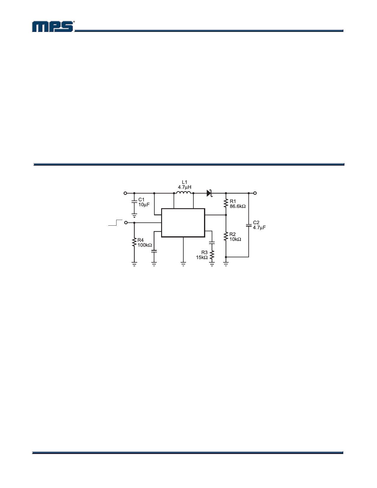
TYPICAL APPLICATION CIRCUIT
D1
VIN
5V
OFF ON
6
5
7
IN
FSEL
SW
2
FB
3
EN
MP3213
8 SS
1
COMP
GND
C4
10nF
4
C3
2.2nF
VOUT
12V
Figure 2—Typical Application Circuit
MP3213 Rev. 1.1
www.MonolithicPower.com
9
5/12/2006
MPS Proprietary Information. Unauthorized Photocopy and Duplication Prohibited.
© 2006 MPS. All Rights Reserved.
Share Link: 