FAN5355 データシートの表示(PDF) - Fairchild Semiconductor
部品番号
コンポーネント説明
一致するリスト
FAN5355 Datasheet PDF : 27 Pages
| |||
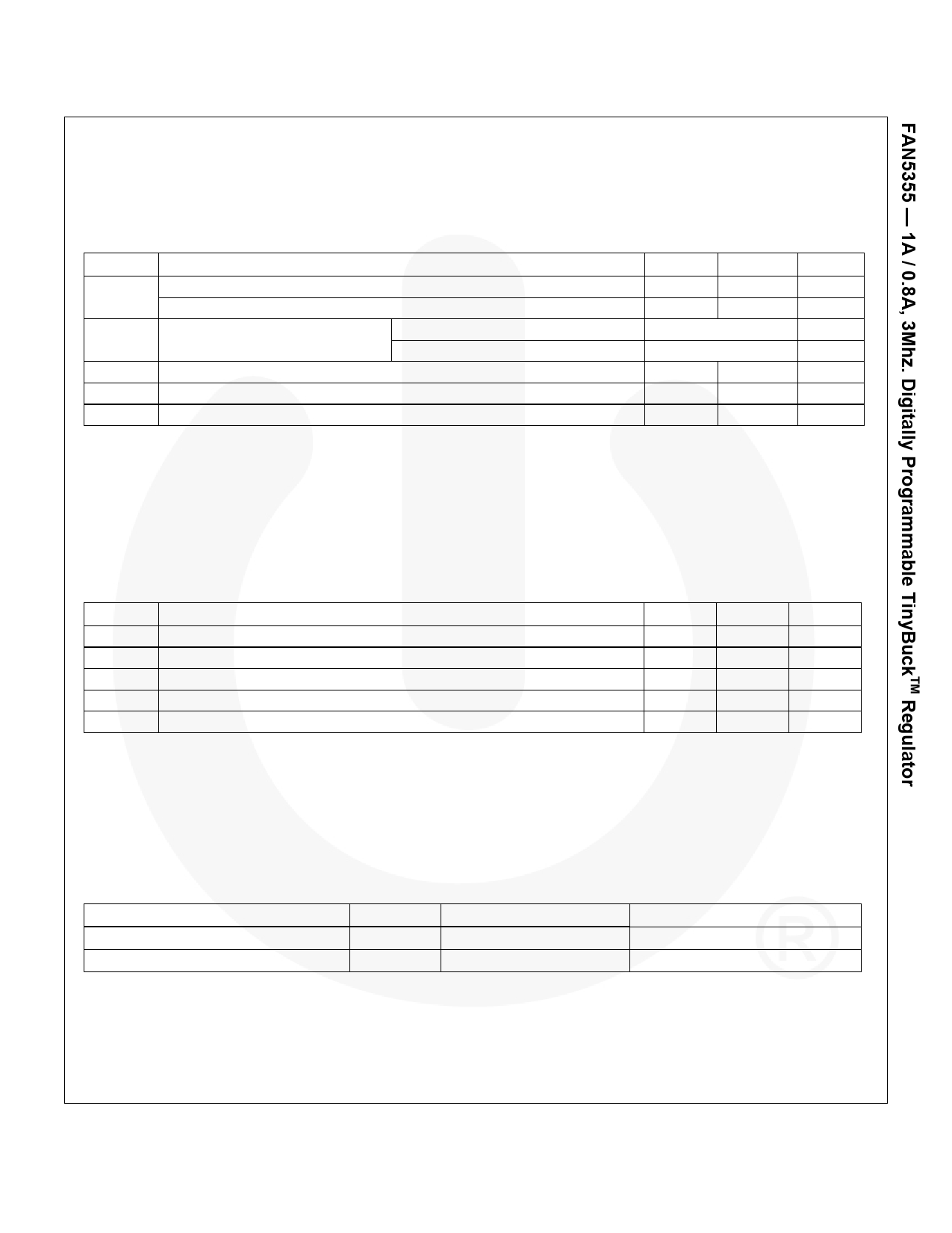
Absolute Maximum Ratings
Stresses exceeding the absolute maximum ratings may damage the device. The device may not function or be operable above
the recommended operating conditions and stressing the parts to these levels is not recommended. In addition, extended
exposure to stresses above the recommended operating conditions may affect device reliability. The absolute maximum ratings
are stress ratings only.
Symbol Parameter
AVIN, SW, PVIN Pins
VCC
Other Pins
ESD
Human Body Model per JESD22-A114
Electrostatic Discharge Protection Level
Charged Device Model per JESD22-C101
TJ
Junction Temperature
TSTG
Storage Temperature
TL
Lead Soldering Temperature, 10 Seconds
Note:
8. Lesser of 6.5V or VCC+0.3V.
Min.
-0.3
-0.3
–40
–65
Max.
6.5
AVIN + 0.3(8)
3.5
1.5
+150
+150
+260
Units
V
V
KV
KV
°C
°C
°C
Recommended Operating Conditions
The Recommended Operating Conditions table defines the conditions for actual device operation. Recommended operating
conditions are specified to ensure optimal performance to the datasheet specifications. Fairchild does not recommend exceeding
them or designing to absolute maximum ratings.
Symbol Parameter
Min.
Max.
Units
VIN
Supply Voltage
2.7
5.5
V
f
Frequency Range
VSW
SDA and SCL Voltage Swing(9)
2.7
3.3
MHz
2.5
V
TA
Ambient Temperature
–40
+85
°C
TJ
Junction Temperature
–40
+125
°C
Note:
9. The I2C interface operates with tHD;DAT = 0 as long as the pull-up voltage for SDA and SCL is less than 2.5V. If voltage
swings greater than 2.5V are required (for example if the I2C bus is pulled up to VIN), the minimum tHD;DAT must be
increased to 80ns. Most I2C masters change SDA near the midpoint between the falling and rising edges of SCL, which
provides ample tHD;DAT .
Dissipation Ratings(10)
Package
Molded Leadless Package (MLP)
Wafer-Level Chip-Scale Package (WLCSP)
RθJA(11)
49ºC/W
110ºC/W
Power Rating at TA ≤ 25°C
2050mW
900mW
Derating Factor > TA = 25ºC
21mW/ºC
9mW/ºC
Notes:
10. Maximum power dissipation is a function of TJ(max), θJA, and TA. The maximum allowable power dissipation at any
allowable ambient temperature is PD = [TJ(max) - TA ] / θJA.
11. This thermal data is measured with high-K board (four-layer board according to JESD51-7 JEDEC standard).
© 2008 Fairchild Semiconductor Corporation
4
FAN5355 • Rev. 1.0.4
www.fairchildsemi.com
Share Link: 