ICS574M データシートの表示(PDF) - Integrated Circuit Systems
部品番号
コンポーネント説明
一致するリスト
ICS574M Datasheet PDF : 4 Pages
| |||
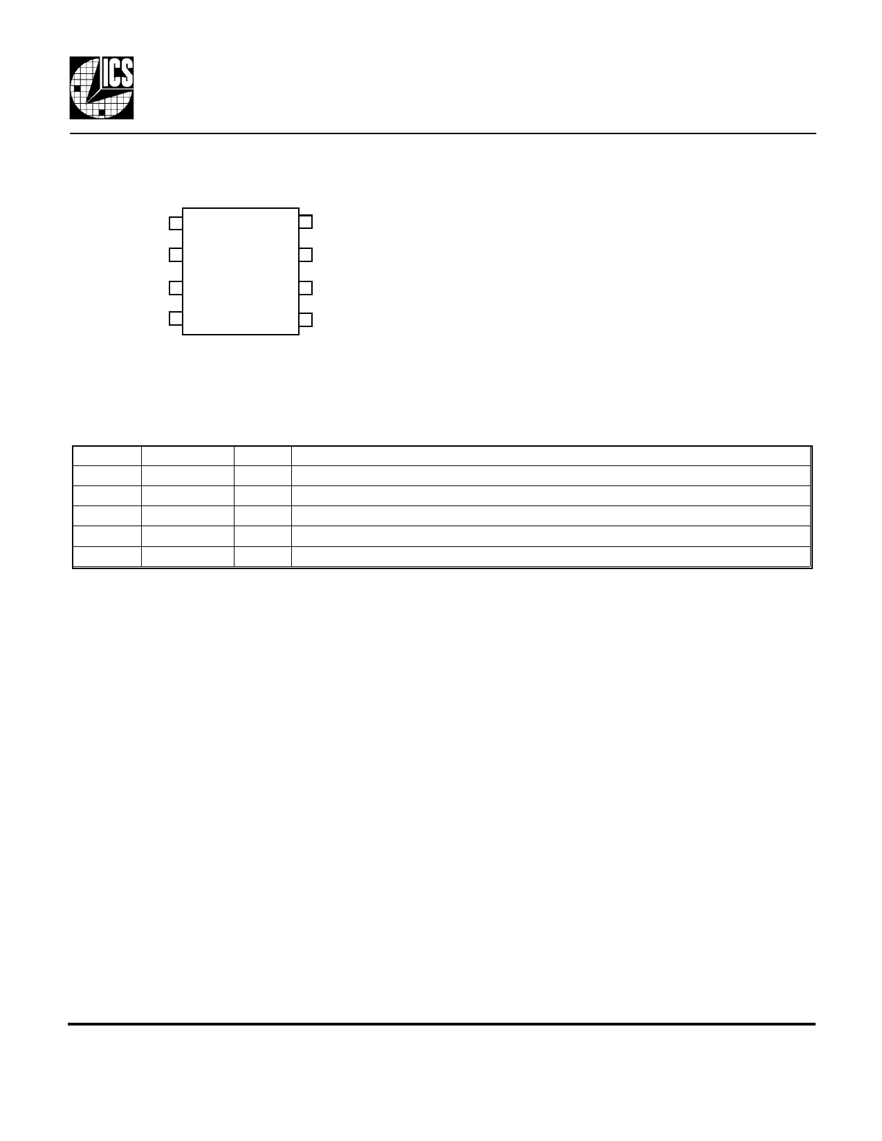
Pin Assignment
CLKIN 1
CLK1 2
CLK2 3
GND 4
8 FBIN
7 CLK4
6 CLK3
5 VDD
Standard 8 pin SOIC
ICS574
Zero Delay, Low Skew Buffer
Pin Descriptions
Number
1
2, 3, 6, 7
5
4
8
Name
CLKIN
CLK1:4
VDD
GND
FBIN
Type
I
O
P
P
I
Description
Clock input. Connect to input clock source.
Four clock outputs.
Power supply. Connect both pins to same voltage (either 3.3V or 5V).
Connect to ground.
Feedback input.
Key: I = Input; O = output; P = power supply connection.
External Components
The ICS574 requires a minimum number of external components for proper operation. Decoupling capacitors of
0.1µF should be connected between VDD and GND on pins 4 and 5, as close to the device as possible. A series
termination resistor of 33 Ω may be used close to the pin for each clock output to reduce reflections.
MDS 574 B
2
Revision 051801
Integrated Circuit Systems, Inc. • 525 Race Street • San Jose • CA • 95126 • (408)295-9800 • www.icst.com
Share Link: 