CS22210 データシートの表示(PDF) - Cirrus Logic
部品番号
コンポーネント説明
一致するリスト
CS22210 Datasheet PDF : 31 Pages
| |||
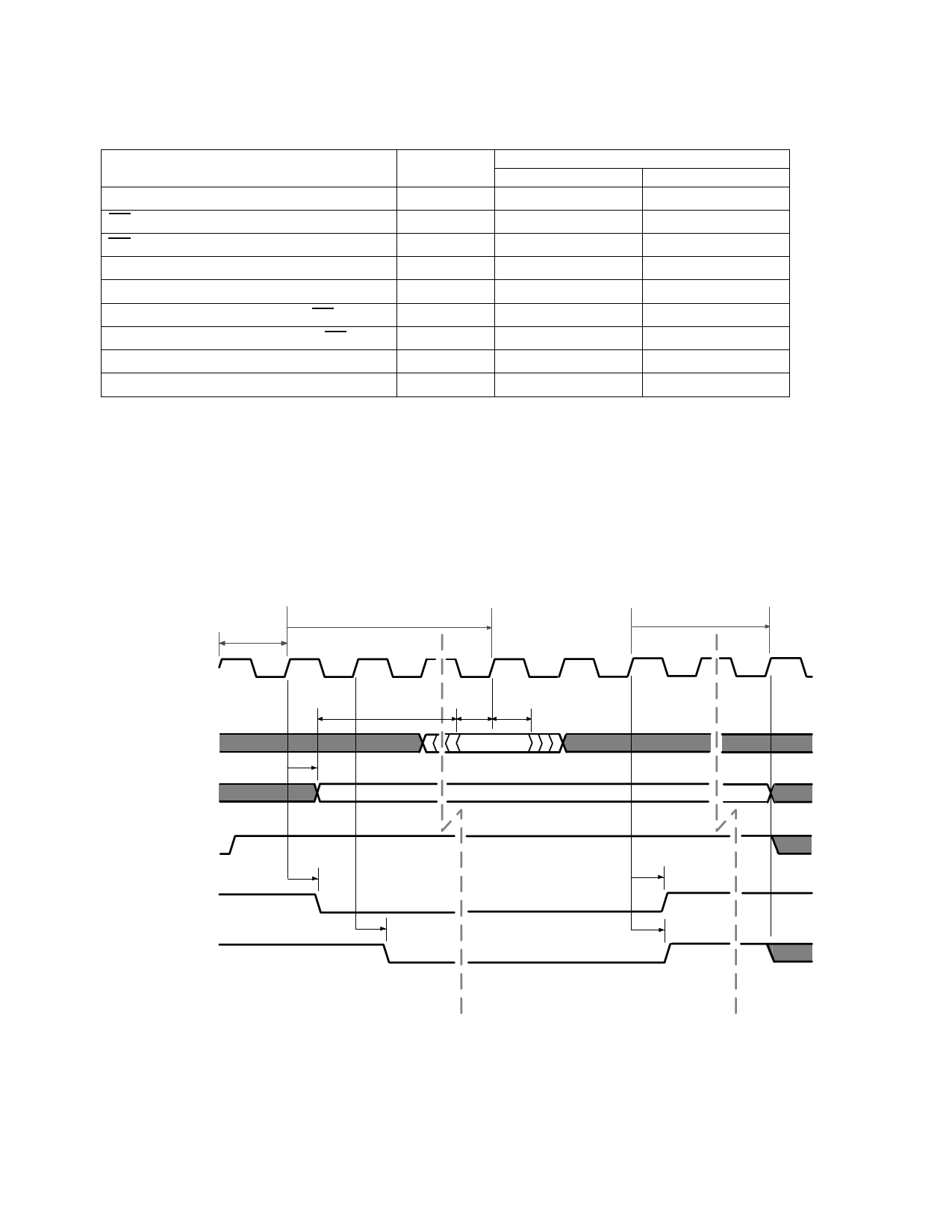
Table 8. ROM/Flash Memory Read Timing
Item
Clock Period (1)
CE to SMD Latched Data (2)
OE de-asserted to OE asserted (3)
ROM address to output delay (4)
SMCLK to SMA output delay
SMCLK to BRCE output delay (CE)
SMCLK to SMRAS output delay (OE)
SMD setup to SMCLK
SMD hold from SMCLK
Symbol
tperSMCLK
tid SMD
tf SMRAS
tACC
td SMA
td BRCE
td SMRAS
tsu SMD
th SMD
Min
72 MHz
6(tperSMCLK)
1.0 ns
2.4 ns
Max
103 MHz
221 ns
220 ns
4.0 ns
4.5 ns
5.0 ns
Notes:
1. The memclock timing is derived by bootstrap PLL settings. Synchronous modes at 77 MHz & 72 MHz are currently
supported.
2. tid SMD is based on the fm_romrdlat register settings – default is 09h max. (77Mhz ~ 17 times SMCLK = 221ns).
3. tf SMRAS is the minimum time required before the next OE is active on the bus (6 times SMCLK). The ROM device
must release the bus within this time frame (77MHz ~ 78 ns).
4. Based on default fm_romrdlat register settings (note: 09h translates to 11h) see fm_romrdlat register settings for more
information).
tpeSr MCLK
SMCLK
SMD[7:0]
SMA[11:0], SMD[13:8]
t ACC
tdSMA
tldSMD
tsSuMD
t
SMD
h
DATA
ADDRESS
SMNWE
BRCE (CE)
SMRAS (OE)
tdBRCE
tdSMRAS
t
SMRAS
f
tdBRCE
tdSMRAS
Figure 7. ROM Memory Interface 'Read' Timing Diagram
CS22210 PCI/USB Wireless Controller
27 of 31
www.cirrus.com
D556PP2 Rev. 3.0
Share Link: 