FX909AD2 データシートの表示(PDF) - CML Microsystems Plc
部品番号
コンポーネント説明
一致するリスト
FX909AD2 Datasheet PDF : 47 Pages
| |||
Wireless Modem Data Pump
FX909A
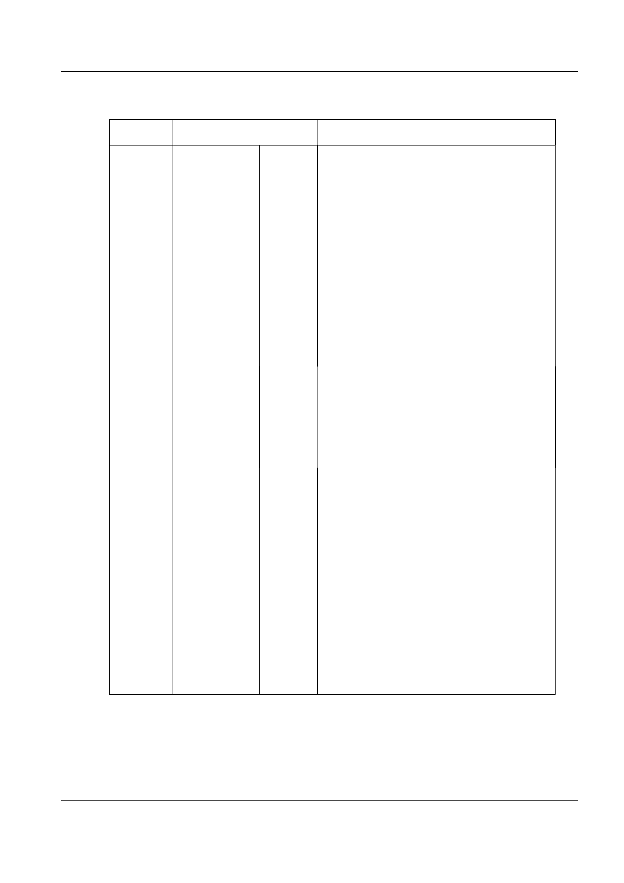
1.3 Signal List
Package
D2/D5/P4
Signal
Description
Pin No.
1
2
3
4
5
6
7
8
9
10
11
12
13
14
15
16
17
18
19
Name
IRQN
D7
D6
D5
D4
D3
D2
D1
D0
RDN
WRN
Vss
CSN
A0
A1
XTALN
XTAL/CLOCK
DOC 2
DOC 1
Type
O/P
BI
BI
BI
BI
BI
BI
BI
BI
I/P
I/P
Power
I/P
I/P
I/P
O/P
I/P
O/P
O/P
A 'wire-ORable' output for connection to the host
µC's Interrupt Request input. This output has a
low impedance pull down to VSS when active
and is high impedance when inactive.
)
)
)
) 8-bit bidirectional 3-state µC interface data
) lines.
)
)
)
Read. An active low logic level input used to
control the reading of data from the modem into
the host µC.
Write. An active low logic level input used to
control the writing of data into the modem from
the host µC.
The negative supply rail (ground).
Chip Select. An active low logic level input to the
modem, used to enable a data read or write
operation.
) Two logic level modem register select
) inputs.
The output of the on-chip oscillator.
The input to the on-chip oscillator, for external
Xtal circuit or clock.
) Connections to the Rx level measurement
) circuitry. A capacitor should be connected
) from each pin to VSS.
© 1996 Consumer Microcircuits Limited
4
D/909A/4
Share Link: 