RF2681 データシートの表示(PDF) - RF Micro Devices
部品番号
コンポーネント説明
一致するリスト
RF2681 Datasheet PDF : 8 Pages
| |||
Preliminary
4
RF2681
W-CDMA LINEAR VARIABLE GAIN
DRIVER AMPLIFIER
Typical Applications
• PA Driver Amplifier for W-CDMA Handsets • General Purpose Driver Amplifier
Product Description
1.00
0.85
3.00
0.80
sq.
The RF2681 is a linear variable gain amplifier specifically
0.65
0.60
designed for PA driver applications in W-CDMA handsets.
0.24 typ
4
0.65
0.30
4 PLCS
The device maintains excellent linearity over a 30dB gain
control range, while providing a maximum of 26dB gain.
The IC is manufactured on an advanced Gallium Ars-
2
0.30
0.18
10..2955sq.
enide Heterojunction Bipolar Transistor Process and is
provided in an extremely small 3mmx3mm, 12-pin, lead-
less chip carrier.
12°
max
0.05
0.01
0.75
0.50
0.50
0.23
0.13
4 PLCS
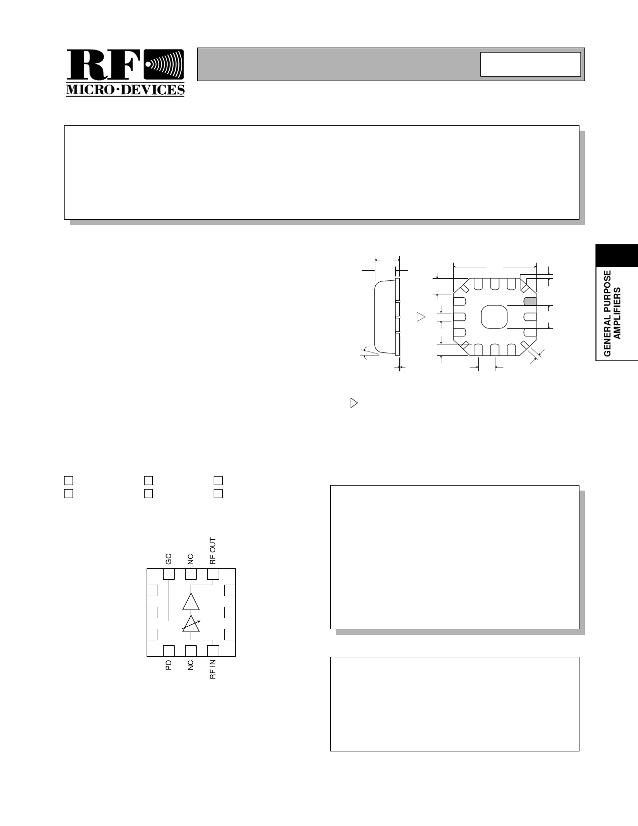
Dimensions in mm.
NOTES:
1 Shaded Pin is Lead 1.
2 Dimension applies to plated terminal and is measured between 0.02 mm and
0.25 mm from terminal end.
3 Pin 1 identifier must exist on top surface of package by identification mark or
feature on the package body. Exact shape and size is optional.
4 Package Warpage: 0.05 mm max.
5 Die thickness allowable: 0.305 mm max.
Optimum Technology Matching® Applied
Si BJT
üGaAs HBT
GaAs MESFET
Si Bi-CMOS
SiGe HBT
Si CMOS
12 11 10
VCC1 1
9 GND
VREG 2
8 GND
VCC2 3
7 GND
456
Package Style: LCC, 12-Pin, 3x3
Features
• 30dB Linear Gain Control Range
• 26dB Maximum Gain
• Single 2.7V to 3.3V Supply
• High Linearity Over Entire Gain Control
Range
• 9dBm Output Drive Available
Ordering Information
RF2681
W-CDMA Linear Variable Gain Driver Amplifier
RF2681 PCBA Fully Assembled Evaluation Board
Functional Block Diagram
RF Micro Devices, Inc.
7628 Thorndike Road
Greensboro, NC 27409, USA
Tel (336) 664 1233
Fax (336) 664 0454
http://www.rfmd.com
Rev A1 010824
4-43
Share Link: 