TEA2014A データシートの表示(PDF) - STMicroelectronics
部品番号
コンポーネント説明
一致するリスト
TEA2014A Datasheet PDF : 4 Pages
| |||
TEA2014A
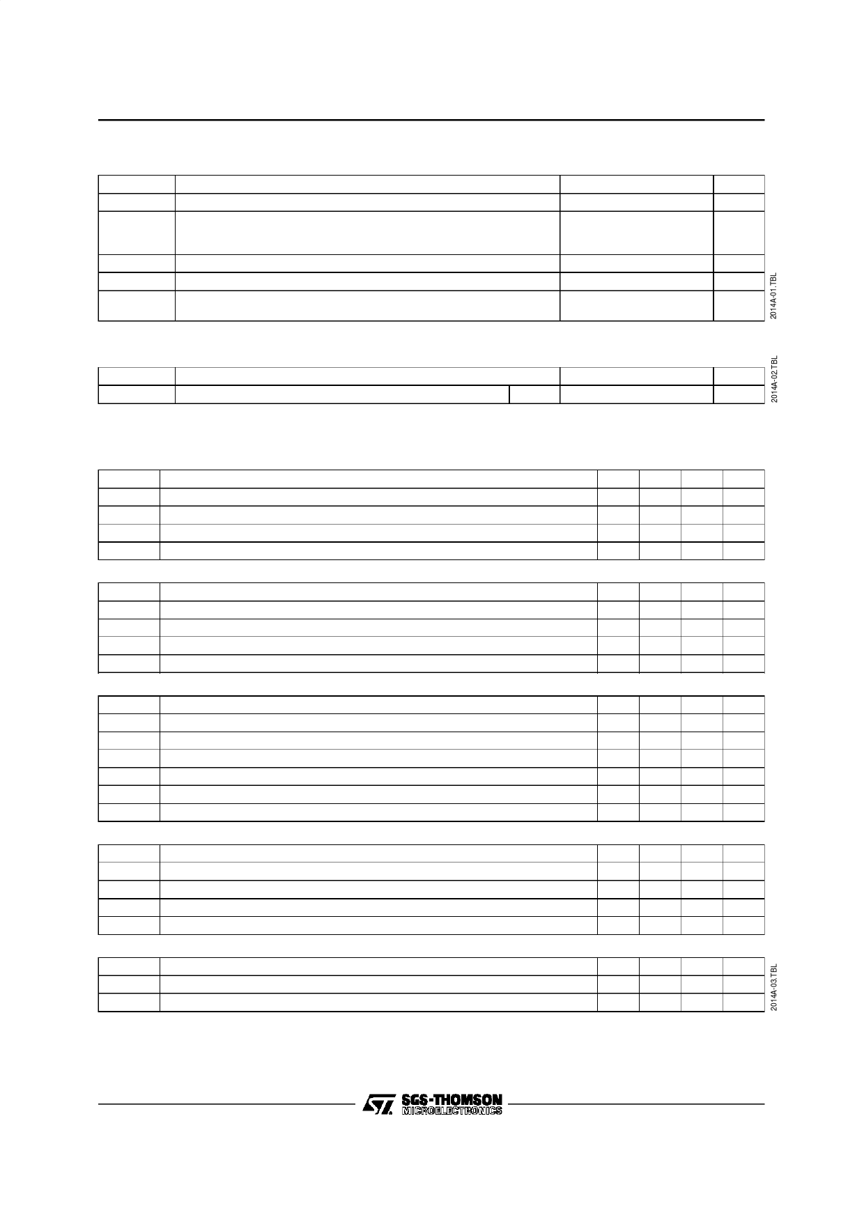
ABSOLUTE MAXIMUM RATINGS
Symbol
VCC
Toper
Tj
Tstg
–
Parameter
Supply Voltage
Operating Temperature
with Load > 150 Ω on PIN 2
with Load = 75 Ω on PIN 2
Junction Temperature
Storage Temperature
Minimum DC Load Resistor PIN 6
Minimum DC Load Resistor PIN 2
Value
Unit
18
V
°C
0, + 100
0, + 70
– 40, + 150
°C
– 40, + 150
°C
600
Ω
75
Ω
THERMAL DATA
Symbol
Rth (j-a)
Parameter
Junction-ambient Thermal Resistance
Value
Unit
Typ.
90
°C/W
ELECTRICAL CHARACTERISTICS
Tamb = + 25 °C, VCC = 9 V (unless otherwise specified)
Symbol
Parameter
VCC Supply Voltage Range
ICC Supply Current (no load on Pin 2 and Pin 6)
ICC Supply Current (with 75 Ω Pin 2.1, with 600 Ω between Pin 6.1)
Ptot Total Power Dissipation with Load
INPUTS (pin 8 and pin 3)
–
Internal Video Input Swing from Picture IF (positive Video)
–
Internal Video Input Impedance (positive video)
–
Internal Video Input Bias Current (positive video)
–
External Video Input Swing (positive video)
–
External Video Input Impedance (positive video)
SWITCHED OUTPUT (pin 6) - RLOAD = 600 Ω
–
Video Output Swing
–
Video Output Dynamic Impedance
–
Video DC Output Voltage (sync. pulse level note 1)
–
Video Bandwith Pin 6 – from Internal Input Pin 3 (– 1 dB)
–
Video Bandwith Pin 6 – from External Input Pin 8 (– 3 dB)
–
Output Gain Pin 6 – Pin 8
–
Output Gain Pin 6 – Pin 3
EXTERNAL OUTPUT (pin 2) - RLOAD = 75 Ω
–
Video Output Swing
–
Video Output Dynamic Impedance
–
Video DC Output Voltage (sync. pulse level , note)
–
Video Bandwidth (– 1dB)
–
Video Output Gain (pin 2 – pin 3)
SWITCHING INPUT (pin 5)
–
Switching Input Unactive Low Level or Unconnected Pin (TV receiving)
–
Switching Input Active Level (ext. receiving)
–
Switching Input Impedance
Note : Use a video signal with a synchro pulse in order to make the clamp work in a correct way.
(75Ω to the ground and 10µF in series).
Min. Typ. Max. Unit
8
– 14 V
–
– 20 mA
– 45 – mA
– 400 – mW
–
– 4.5 Vpp
50 –
– kΩ
6 25 40 µA
–
–
2 Vpp
50 –
– kΩ
4
–
– Vpp
–
– 25 Ω
1.7 2 2.4 V
6
–
– MHz
6
–
– MHz
+ 5 + 6 + 7 dB
– 1 – 0.5 0 dB
2.2 –
– Vpp
–
10
–
Ω
1.7 2 2.4 V
6
–
– MHz
– 1.8 – 1 – 0.4 dB
0
–
3
V
7
– VCC V
10 –
– kΩ
2/4
Share Link: 