TK75018DCTL データシートの表示(PDF) - Toko America Inc
部品番号
コンポーネント説明
一致するリスト
TK75018DCTL Datasheet PDF : 8 Pages
| |||
TK75018
PIN DESCRIPTIONS (CONT.)
INPUT CAPACITOR CHARGING PINS (CAP+/CAP- )
The positive driving pin of CIN (CAP +) charges the positive
node of the capacitor to VIN during tCH and pulls it down to
ground during tDIS. The negative driving pin of CIN
(CAP -) pulls the negative node of the capacitor to ground
during tCH and is driven into the output during tDIS.
CIRCUIT GROUND (GND)
All potentials are referenced to this ground unless otherwise
noted.
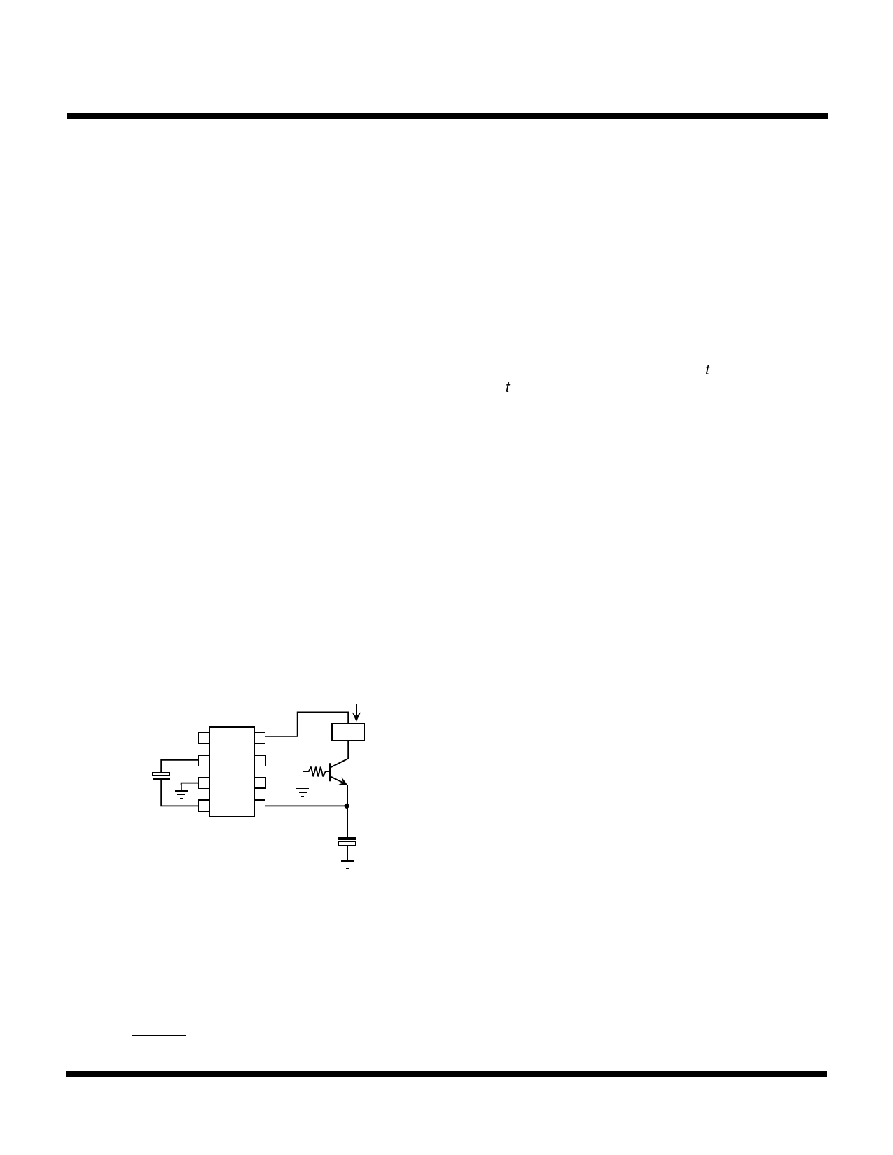
OUTPUT VOLTAGE (VOUT)
In most applications, a capacitor must be placed from this
pin to ground to integrate the charge pulses delivered by
CIN. A minimum of ten times CIN is recommended. Since
the output voltage serves as the substrate inside the IC,
the design must ensure that this pin is never raised to a
higher potential than ground. This phenomenon will tend to
occur when a positive-supply-to-negative-supply load is
present at the converter output. A circuit, such as the one
shown in Figure 4, is recommended. Under normal
operation, the transistor will appear as a short circuit. But
the sink current will be cut off from the output pin if the
voltage starts to approach ground. The resistor is chosen
to keep the transistor saturated under all steady-state
operating conditions.
V+
IL
LOAD
V+
+
CIN
CAP +
GND
CAP - VOUT
COUT
+
FIGURE 4: POSITIVE REFERENCED LOAD
The equation below can be used to calculate the values of
the feedback resistors (R1 and R2) needed to achieve a
desired output voltage.
( ) R2 = R1
|VOUT|
1.2 V
+1
where R1 ≥ 24 kΩ
REFERENCE VOLTAGE (Vref)
This pin provides a nominal 2.5 V buffered reference for
external use. Normal output current should be kept below
~160 µA.
OSCILLATOR PROGRAMMING (OSC)
This pin can be used to alter the nominal 25 kHz frequency
of the internal oscillator. An internal timing capacitor of
~150 pF is alternately charged during tCH and discharged
during tDIS with a 7 µA current source to fixed threshold
levels. Adding an external capacitor from the OSC pin to
ground will parallel the 150 pF capacitor to slow down the
clock period. Adding a small external capacitor from the
OSC pin to the CAP+ pin will source/sink extra charge into/
out-of the internal timing capacitor to speed up the transition
between thresholds and thereby raise the oscillator
frequency. It is recommended that, in the latter
configuration, the capacitor be kept below ~30 pF.
Synchronization of multiple TK75018s can be accomplished
by adding pull-up resistors from the OSC pin to the
reference voltage and using an open collector from an
NPN transistor to provide the discharge. The NPN is then
driven by a clocking pulse, and the same pulse can be
used to drive multiple devices in the same configuration.
It is not recommended to pull the OSC pin high with a low-
impedance source. To synchronize and regulate with
multiple devices, an external reference can be used as the
reference point for the error voltage divider, thus allowing
the internal reference to be used as the pull-up point for the
OSC pin.
INPUT VOLTAGE (V+)
The input voltage is used to charge CIN during the time tCH
during each clock period. CIN is then discharged into the
output capacitor during time tDIS. During tCH, the input
current will be approximately 2.2 times the output current.
During tDIS, the input current will be approximately 0.2
times the output current. A low ESR bypass capacitor will
average out the varying current seen by the input supply -
yielding an average input current of approximately 1.1
times the output current. The bypass capacitor should be
placed as near to the TK75018 as possible to disallow
inductive spikes on the supply rail of the IC. A minimum of
2 µF is recommended.
May 1999 TOKO, Inc.
Page 7
Share Link: 