W210H データシートの表示(PDF) - Cypress Semiconductor
部品番号
コンポーネント説明
一致するリスト
W210H Datasheet PDF : 14 Pages
| |||
W210
Writing Data Bytes
Each bit in the data bytes controls a particular device function
except for the “reserved” bits, which must be written as a logic
0. Bits are written MSB (most significant bit) first, which is bit
7. Table 5 gives the bit formats for registers located in Data
Bytes 0–7.
Table 6 details additional frequency selections that are avail-
able through the serial data interface.
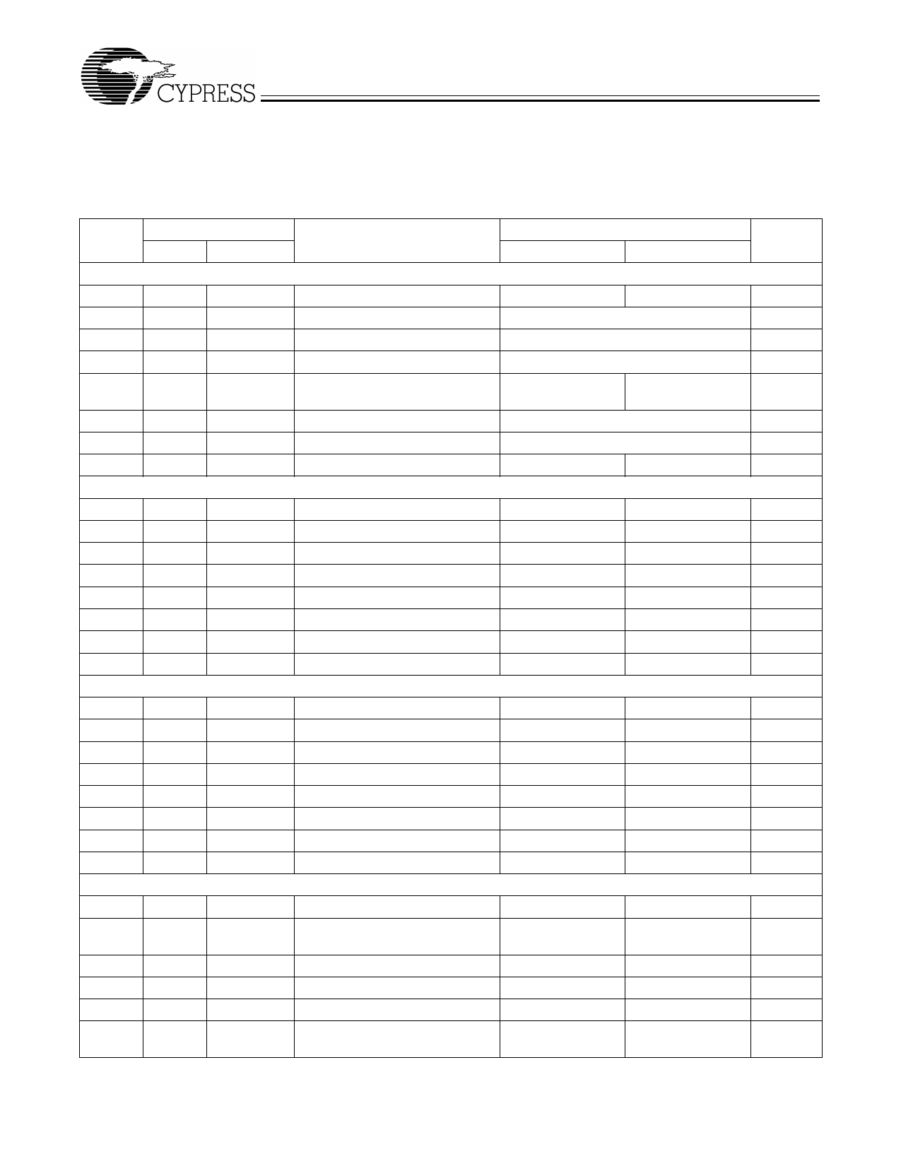
Table 5. Data Bytes 0–7 Serial Configuration Map
Affected Pin
Bit(s) Pin No. Pin Name
Control Function
Data Byte 0
7
--
--
(Reserved)
6
--
--
SEL_2
5
--
--
SEL_1
4
--
--
SEL_0
3
--
--
Hardware/Software Frequency
Select
2
--
--
SEL_4
1
--
--
SEL_3
0
--
--
(Reserved)
Data Byte 1
7
--
--
(Reserved)
6
--
--
(Reserved)
5
--
--
(Reserved)
4
--
--
(Reserved)
3
--
--
(Reserved) Write to ‘1’
2
--
--
(Reserved) Write to ‘1’
1
--
--
(Reserved) Write to ‘1’
0
--
(Reserved) Write to ‘1’
Data Byte 2
7
--
--
(Reserved)
6
7
PCI0
Clock Output Disable
5
--
--
(Reserved)
4
13
PCI5
Clock Output Disable
3
12
PCI4
Clock Output Disable
2
11
PCI3
Clock Output Disable
1
10
PCI2
Clock Output Disable
0
8
PCI1
Clock Output Disable
Data Byte 3
7
--
--
(Reserved)
6
--
SEL_48MHz SEL_48MHz as the output fre-
quency for 24_48MHz
5
26
48MHz Clock Output Disable
4
25
24_48MHz Clock Output Disable
3
--
--
(Reserved)
2
21, 20, SDRAM8:11 Clock Output Disable
18, 17
Bit Control
0
1
--
--
See Table 6
See Table 6
See Table 6
Hardware
Software
See Table 6
See Table 6
Normal
Three-stated
--
--
--
--
--
--
--
--
--
--
--
--
--
--
--
--
--
--
Low
Active
--
--
Low
Active
Low
Active
Low
Active
Low
Active
Low
Active
--
24 MHz
Low
Low
--
Low
--
48 MHz
Active
Active
--
Active
Default
0
0
0
0
0
1
0
0
0
0
0
0
1
1
1
1
0
1
0
1
1
1
1
1
0
0
1
1
0
1
6
Share Link: 